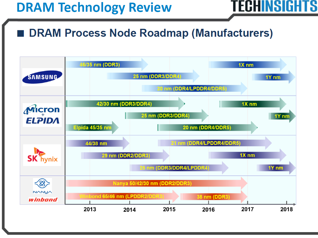
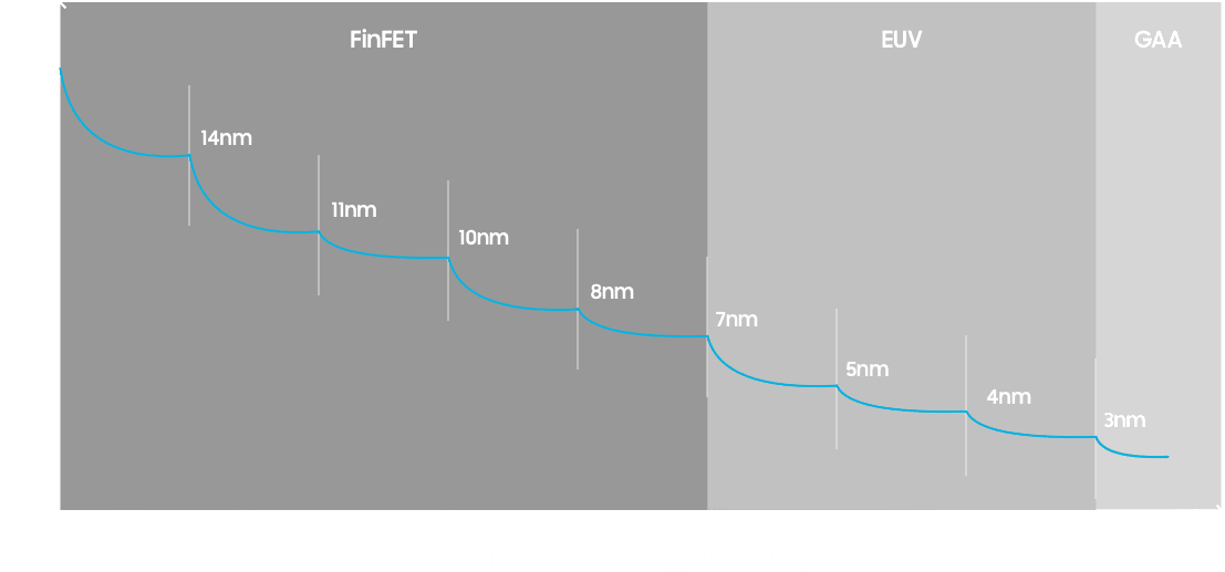
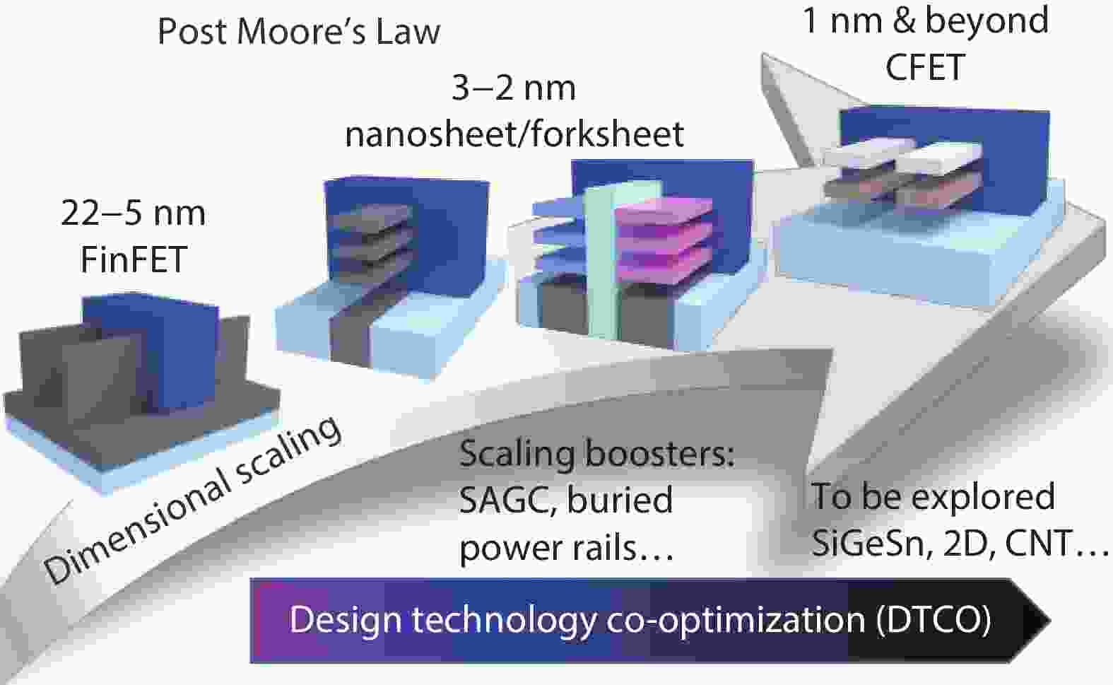
Process Node Technology


![What Are Semiconductor Process Nodes? [Definitive Guide] - Tech4Gamers](https://tech4gamers.com/wp-content/uploads/2024/01/HOW-TO.jpg)


![[Electronics] 3D structural analysis of a 7 nm process nodes SRAM - YouTube](https://i.ytimg.com/vi/nnb6uU0xLQc/maxresdefault.jpg)

![[News] The Imminent Arrival of 2-Nanometer Advanced Process](https://img.trendforce.com/blog/wp-content/uploads/2023/09/20113557/%E6%99%B6%E5%9C%93%E4%BB%A3%E5%B7%A5%E5%BB%A0%E5%85%88%E9%80%B2%E8%A3%BD%E7%A8%8B%E8%B7%AF%E7%B7%9A%E5%9C%96_ENG.png)


![TSMC Logic Node [1]. | Download Scientific Diagram](https://www.researchgate.net/publication/361681530/figure/fig1/AS:11431281095923693@1668053329933/TSMC-Logic-Node-1.png)


![What Are Semiconductor Process Nodes? [Definitive Guide] - Tech4Gamers](https://tech4gamers.com/wp-content/uploads/2023/07/Intel-Core-i9-13900K.jpg)


![[News] Progress and Adoption of Advanced Processes by Samsung, Intel ...](https://img.trendforce.com/blog/wp-content/uploads/2023/09/20113557/%E6%99%B6%E5%9C%93%E4%BB%A3%E5%B7%A5%E5%BB%A0%E5%85%88%E9%80%B2%E8%A3%BD%E7%A8%8B%E8%B7%AF%E7%B7%9A%E5%9C%96_ENG-624x327.png)

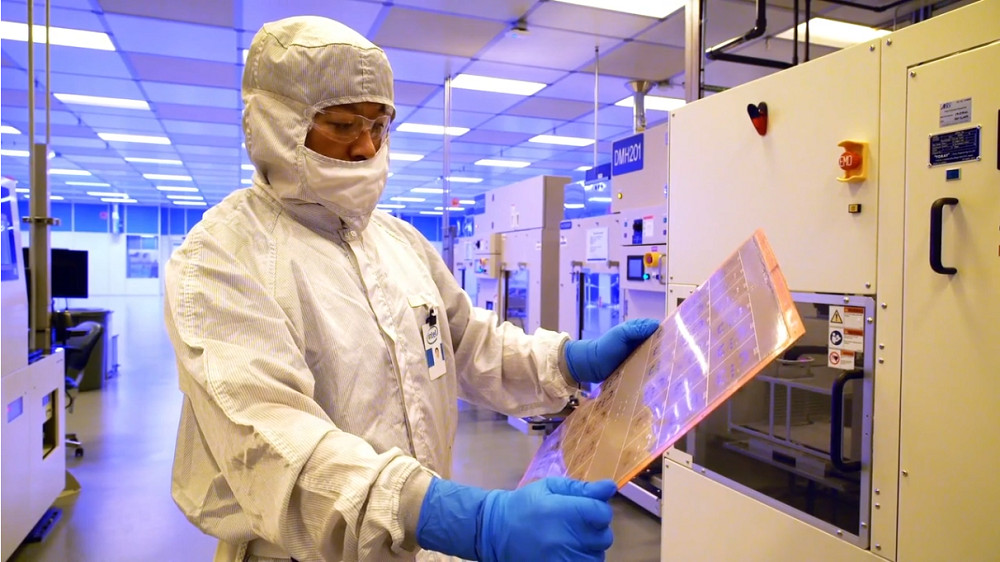
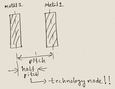
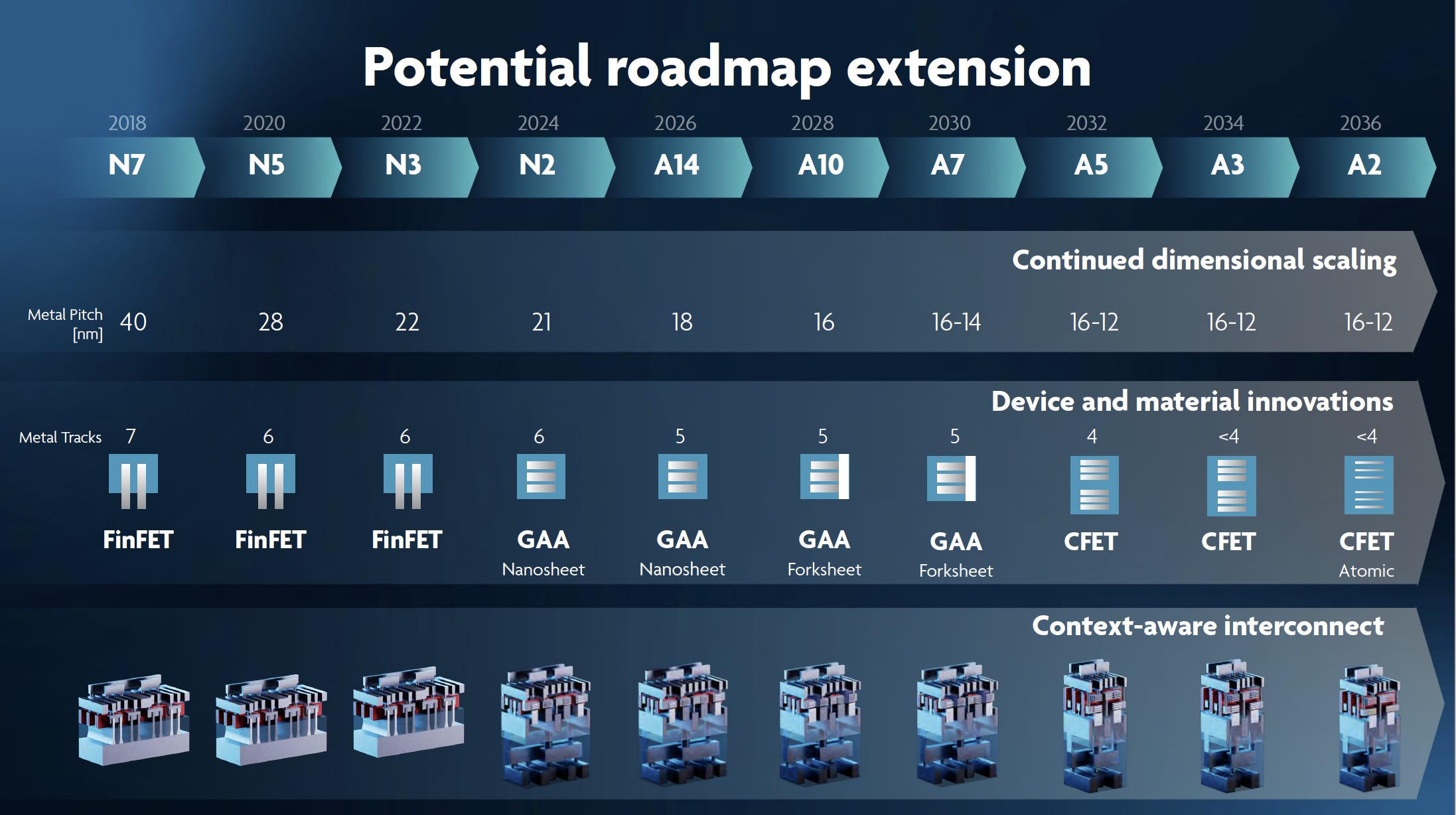
Live your best life through countless lifestyle-focused Process Node Technology photographs. encouraging positive living via computer, digital, and electronic. ideal for wellness and self-improvement content. The Process Node Technology collection maintains consistent quality standards across all images. Suitable for various applications including web design, social media, personal projects, and digital content creation All Process Node Technology images are available in high resolution with professional-grade quality, optimized for both digital and print applications, and include comprehensive metadata for easy organization and usage. Discover the perfect Process Node Technology images to enhance your visual communication needs. Whether for commercial projects or personal use, our Process Node Technology collection delivers consistent excellence. Advanced search capabilities make finding the perfect Process Node Technology image effortless and efficient. Professional licensing options accommodate both commercial and educational usage requirements. Time-saving browsing features help users locate ideal Process Node Technology images quickly. Diverse style options within the Process Node Technology collection suit various aesthetic preferences. The Process Node Technology collection represents years of careful curation and professional standards. Reliable customer support ensures smooth experience throughout the Process Node Technology selection process. Cost-effective licensing makes professional Process Node Technology photography accessible to all budgets. Each image in our Process Node Technology gallery undergoes rigorous quality assessment before inclusion.