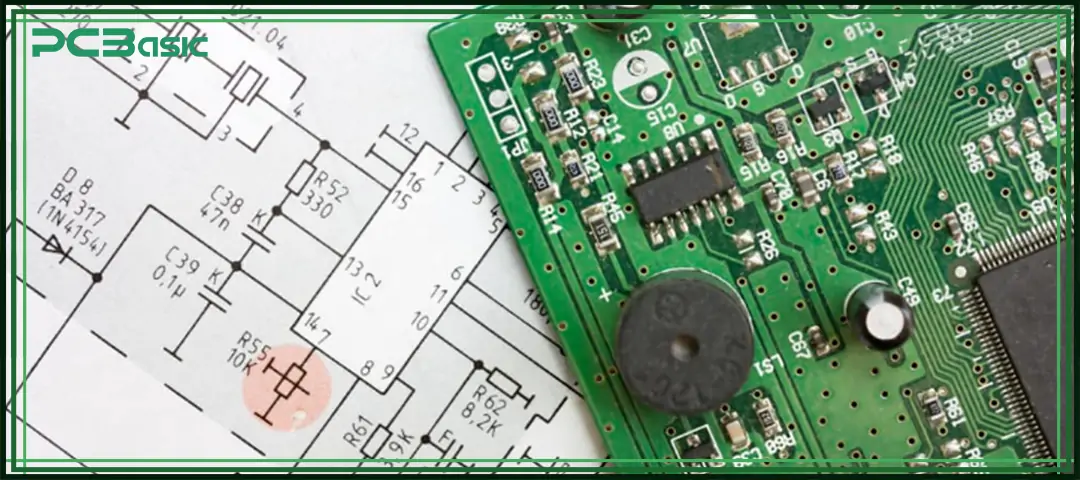
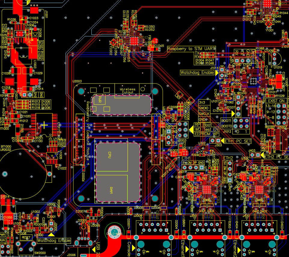
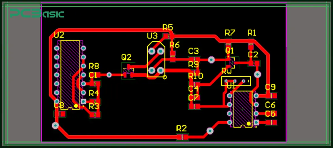
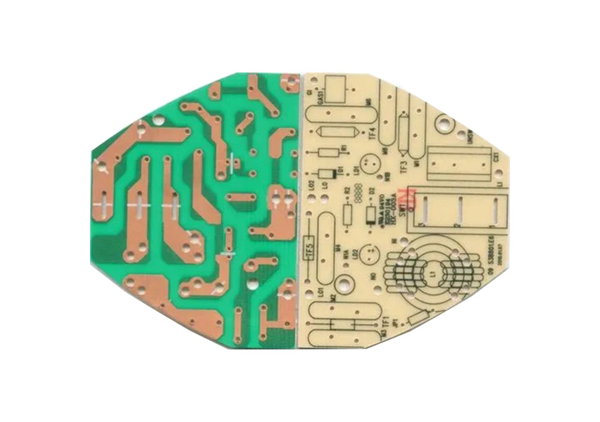
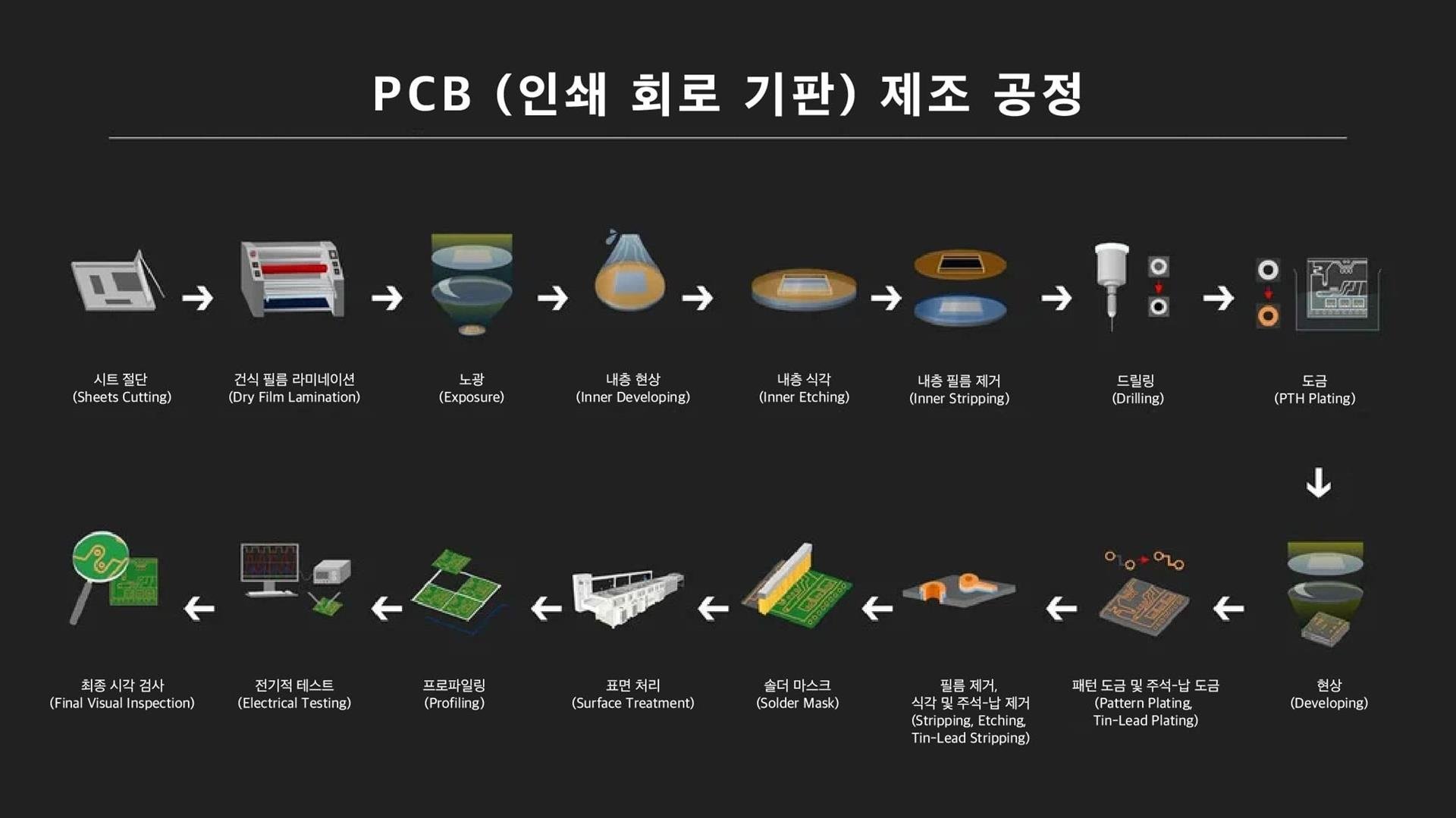
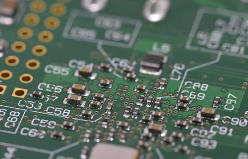
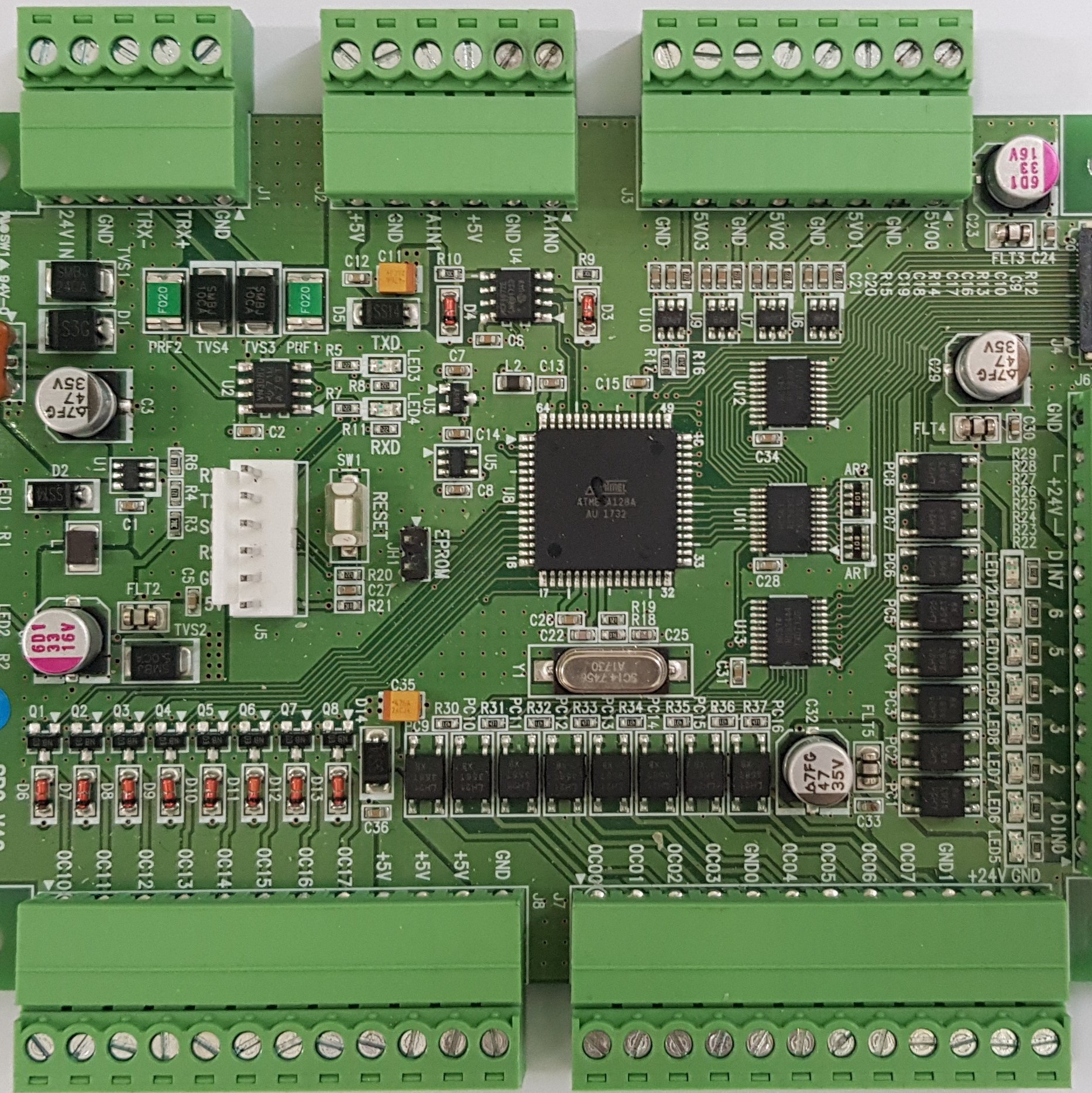
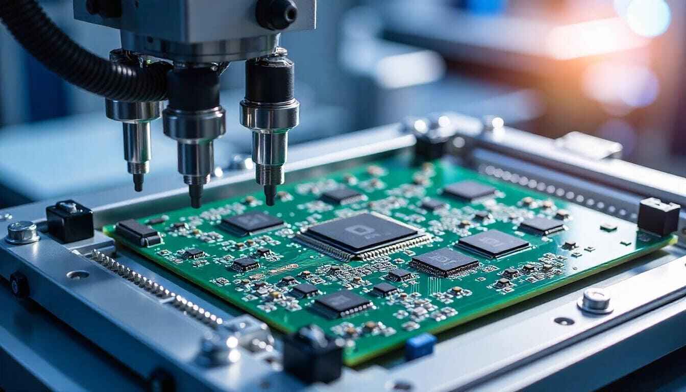
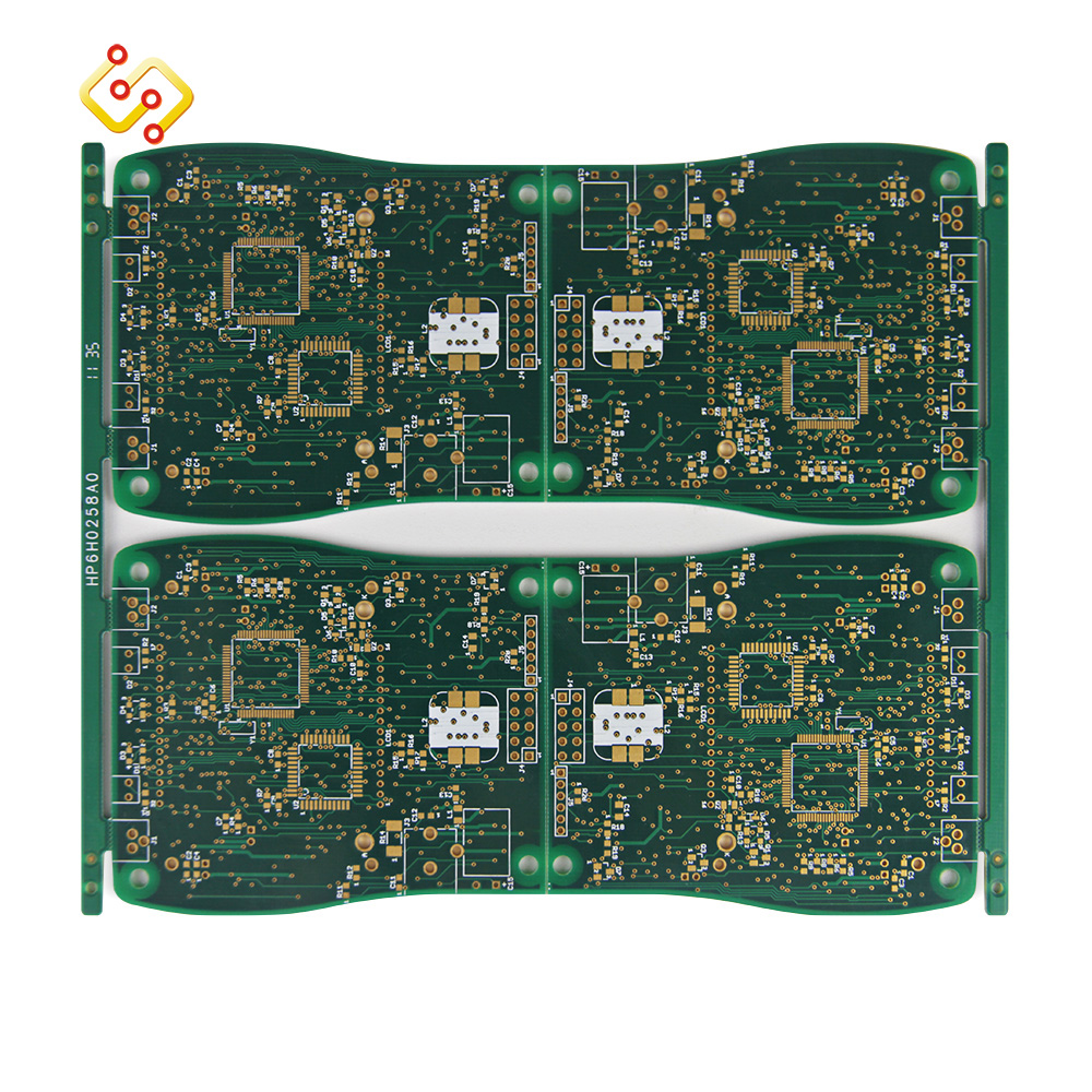
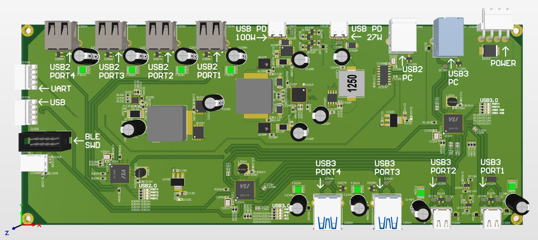
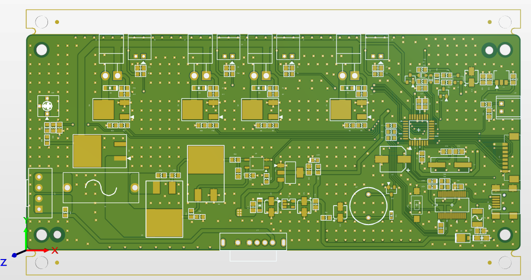
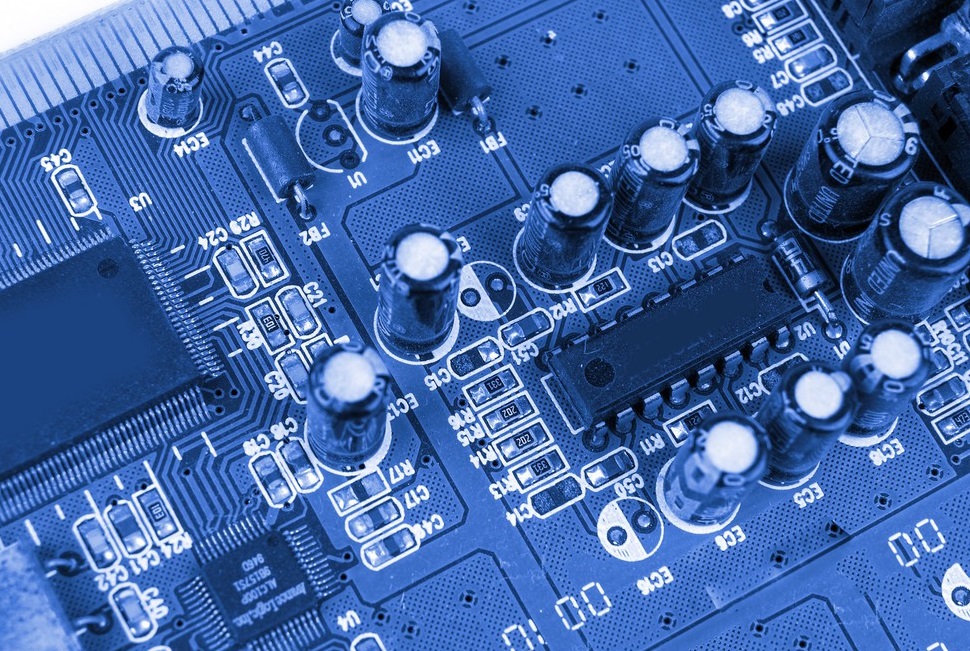
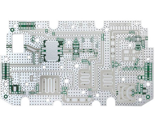
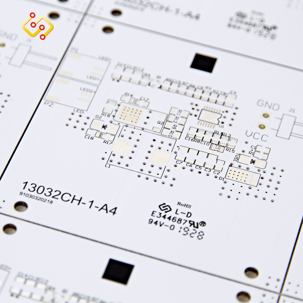
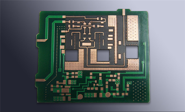
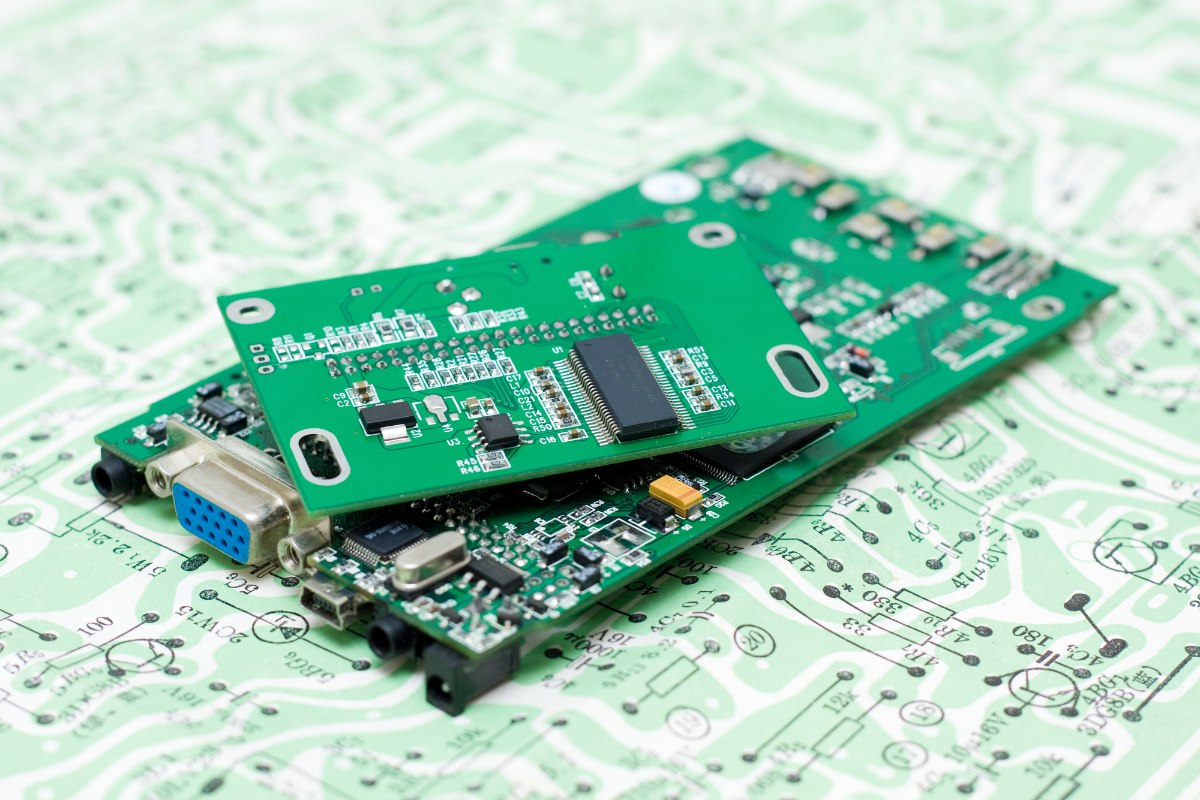
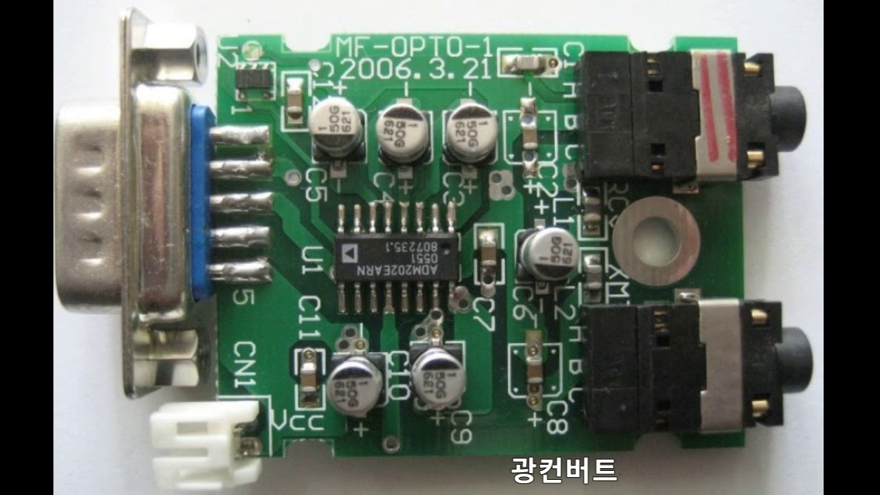
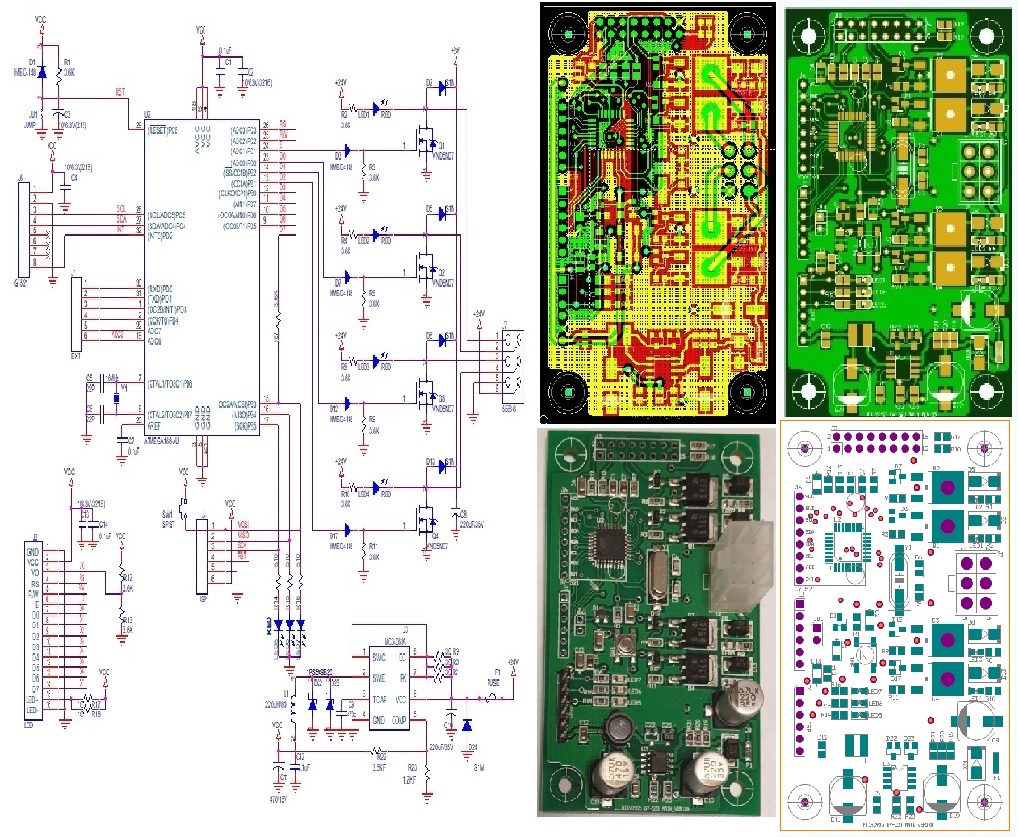
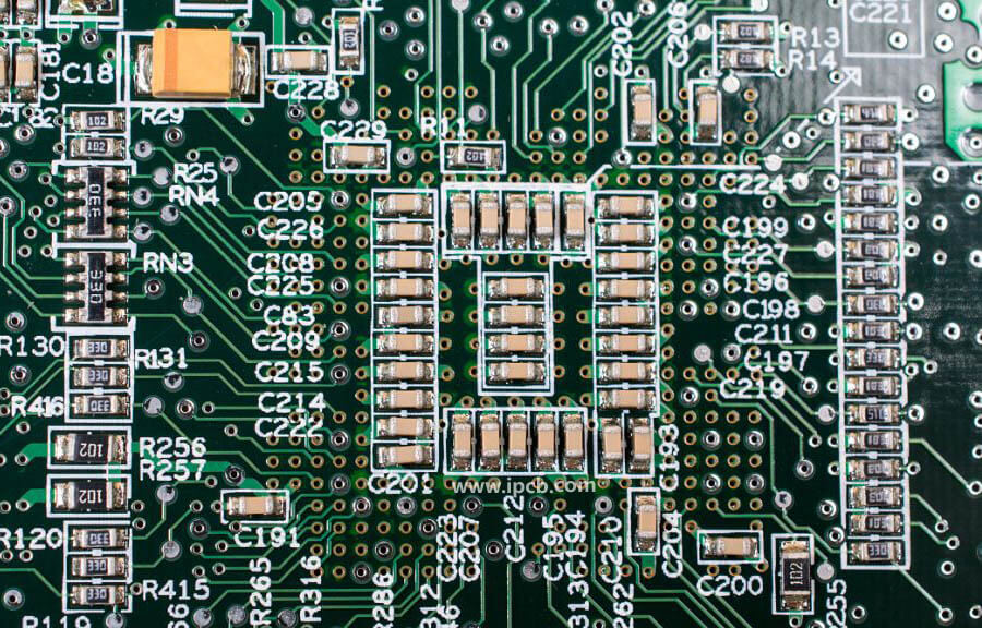
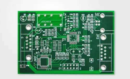
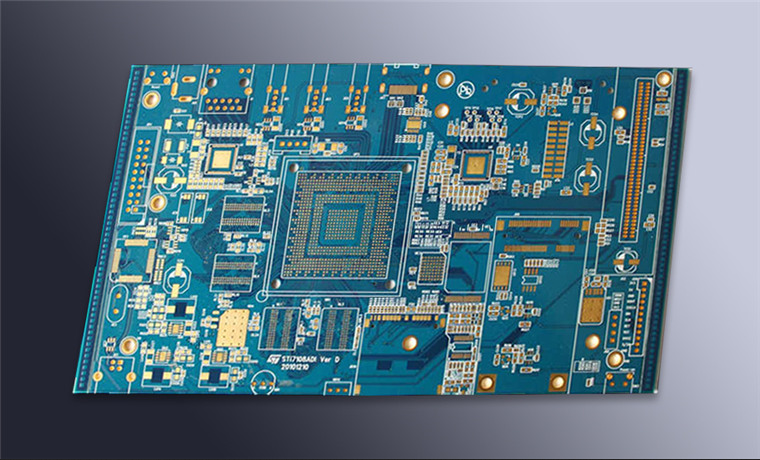
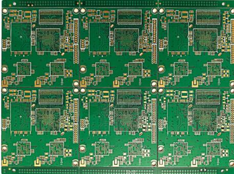
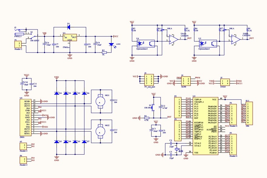
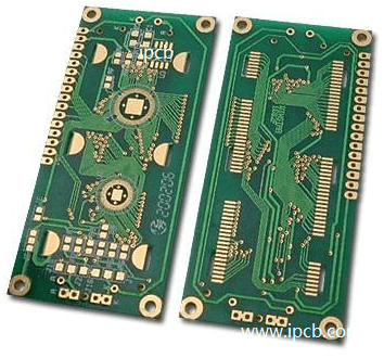
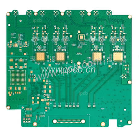
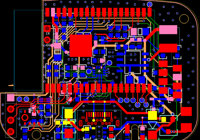
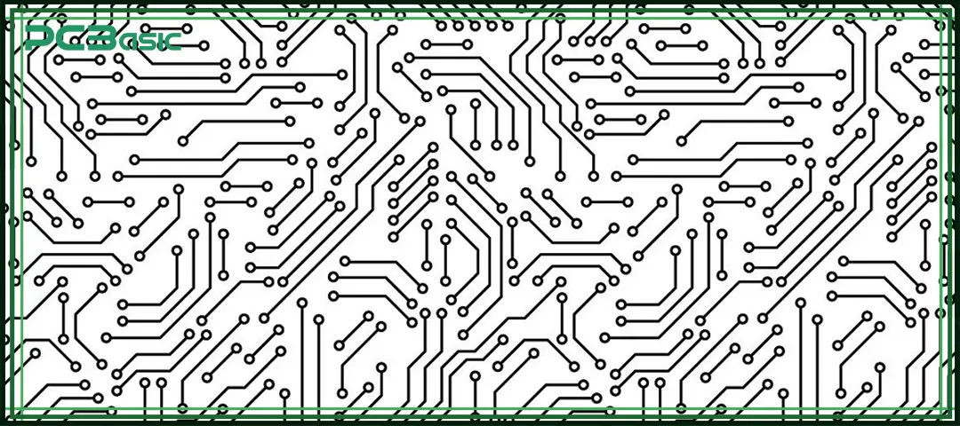
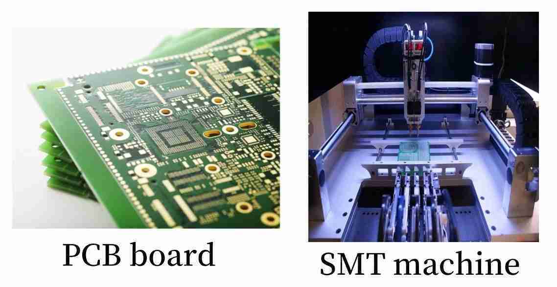
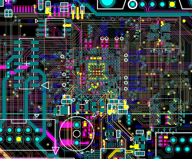
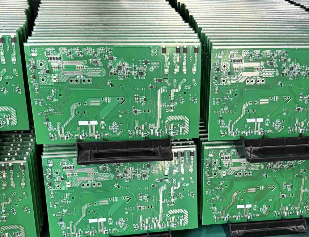
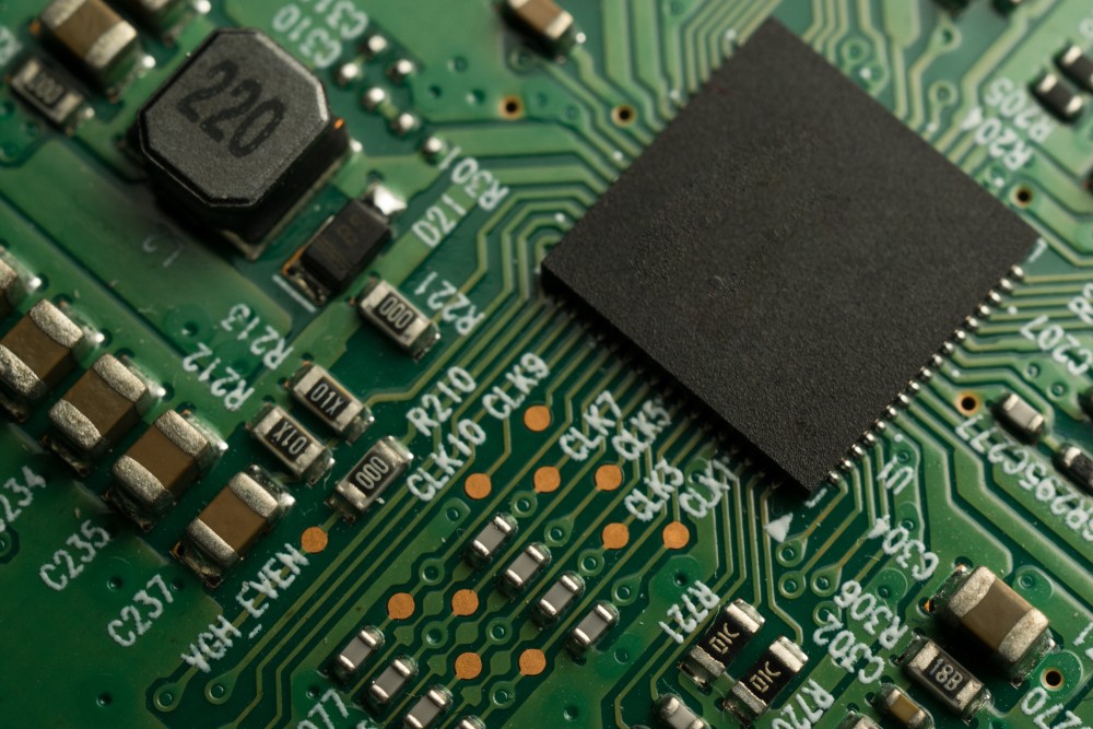
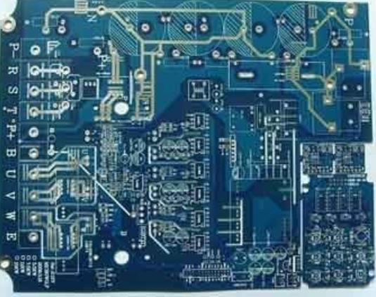
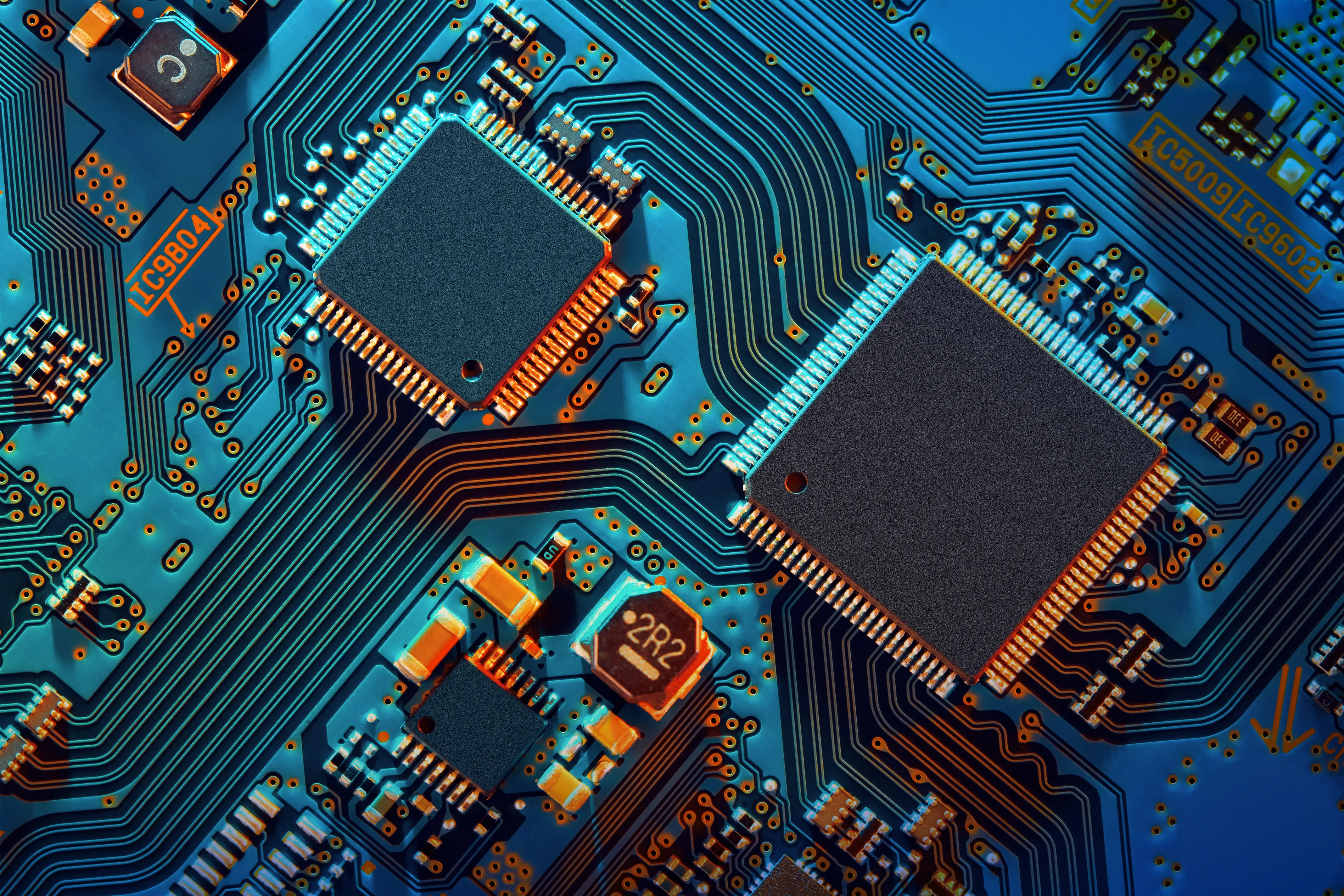
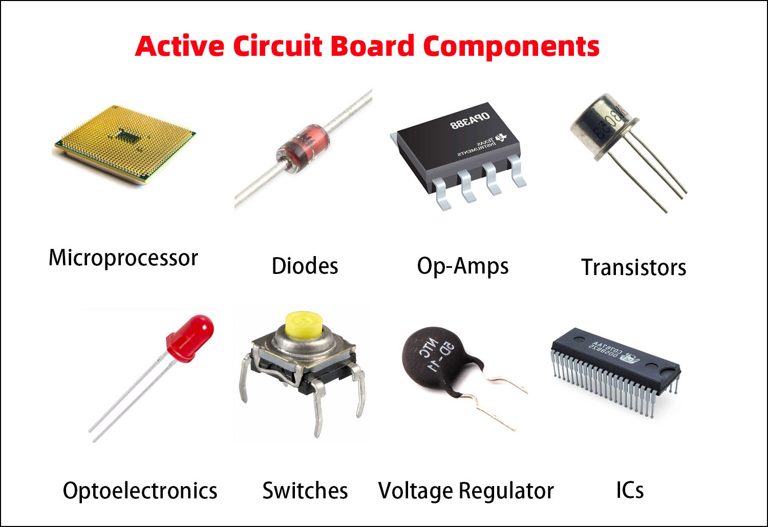
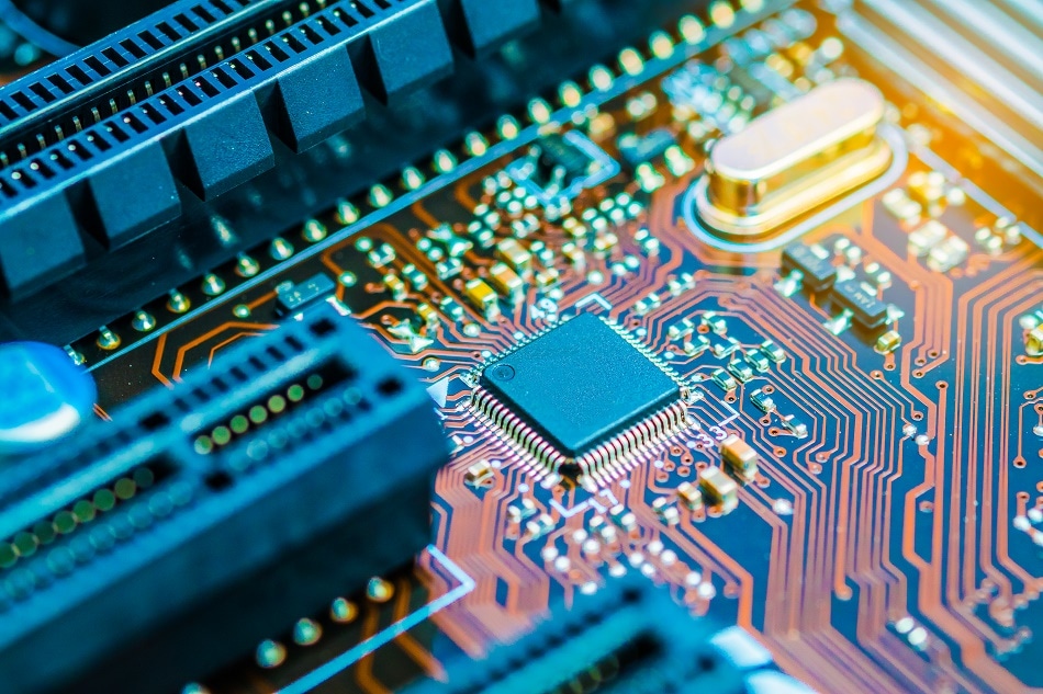
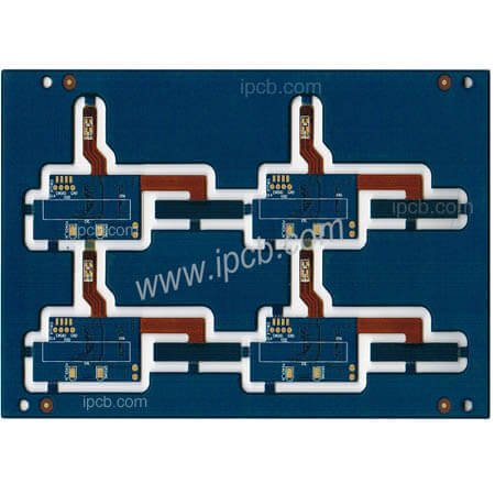
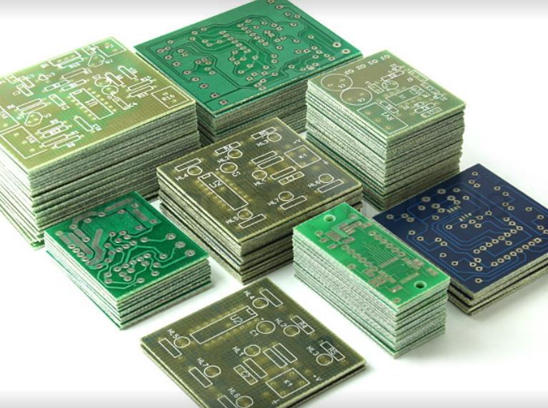
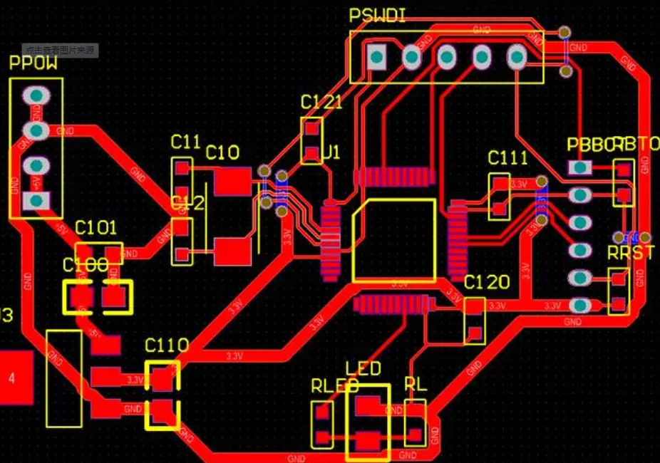
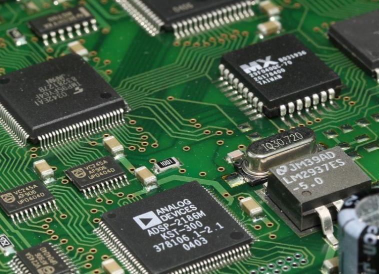
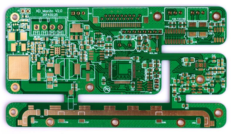
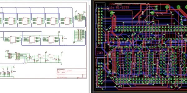
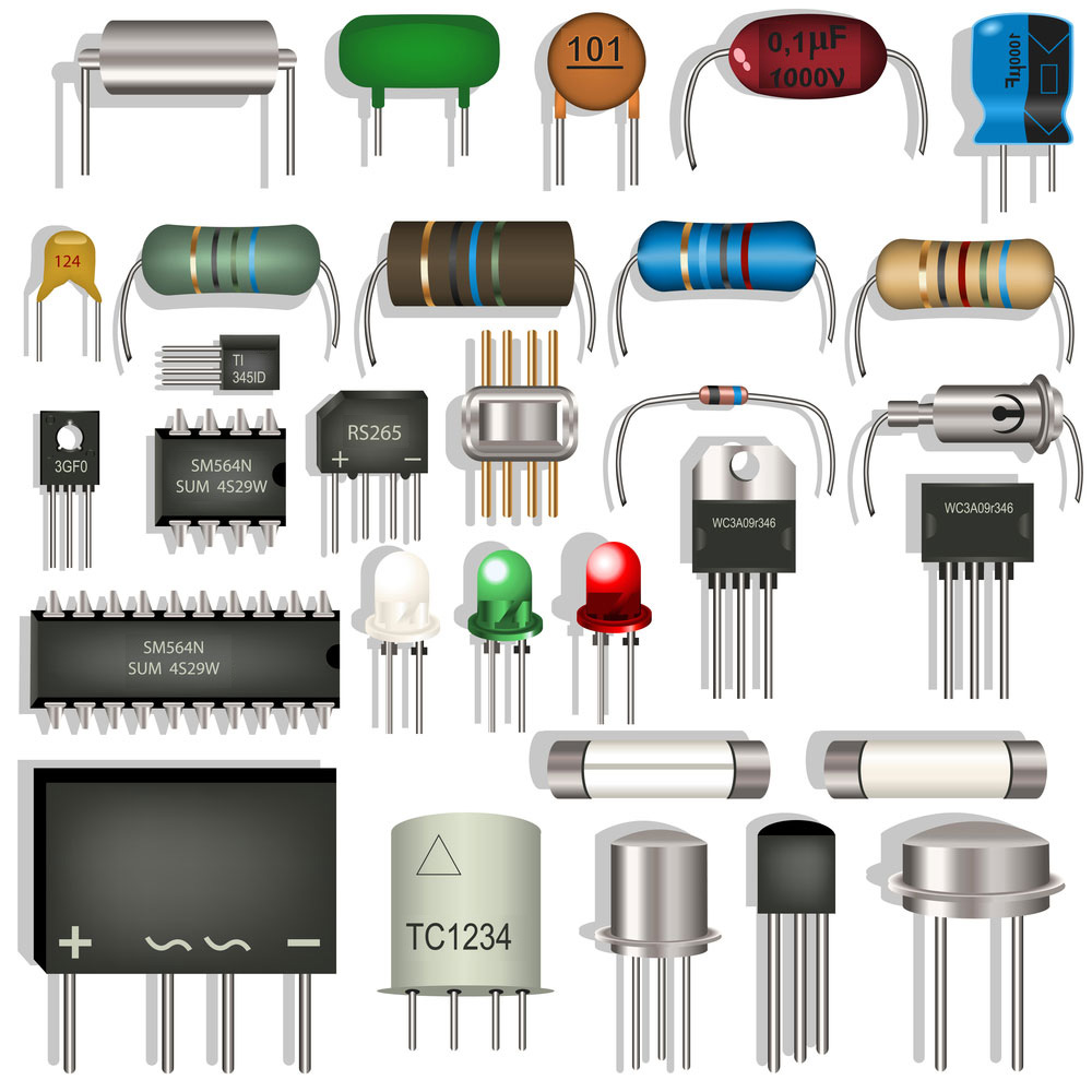
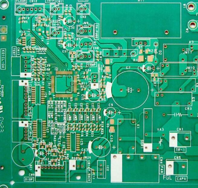
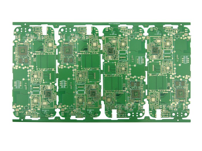
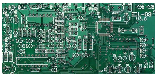
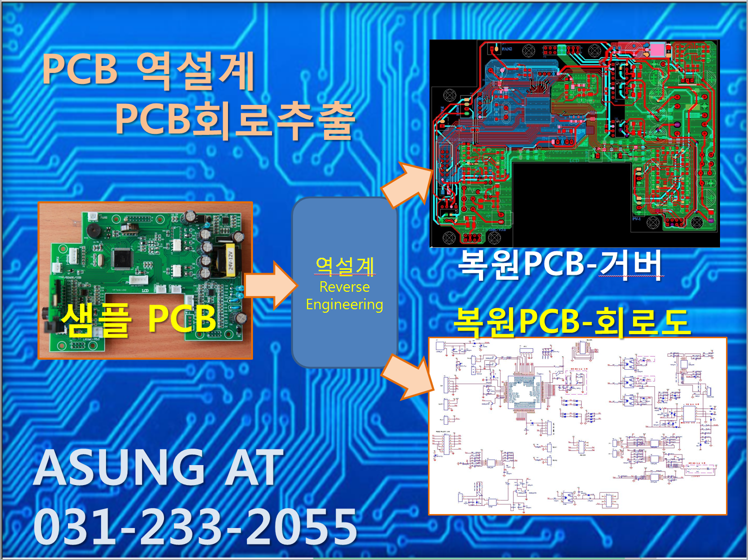
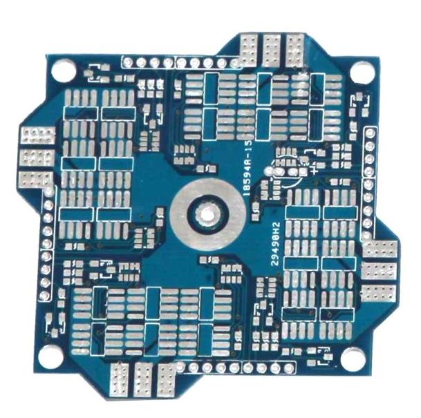
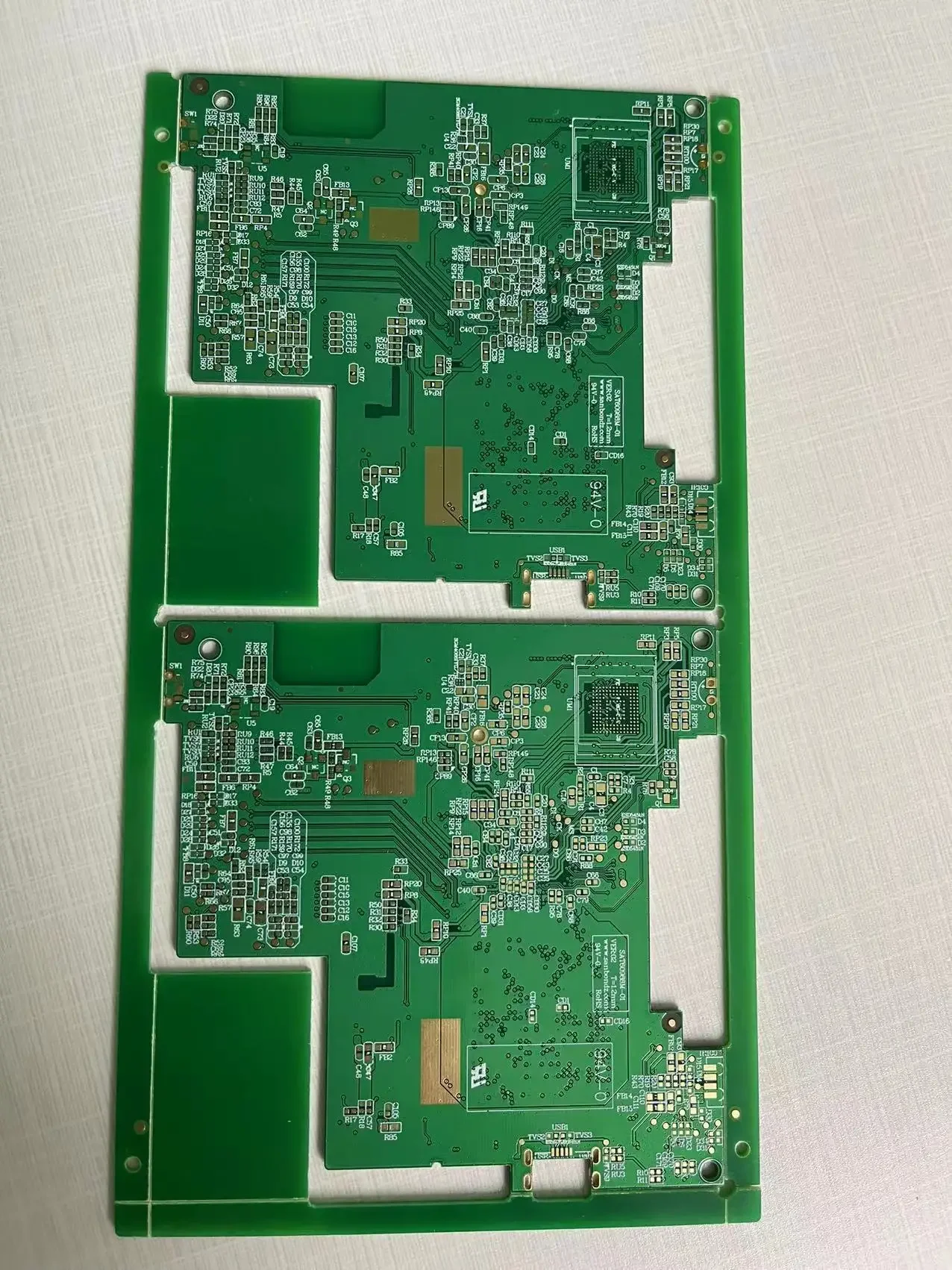
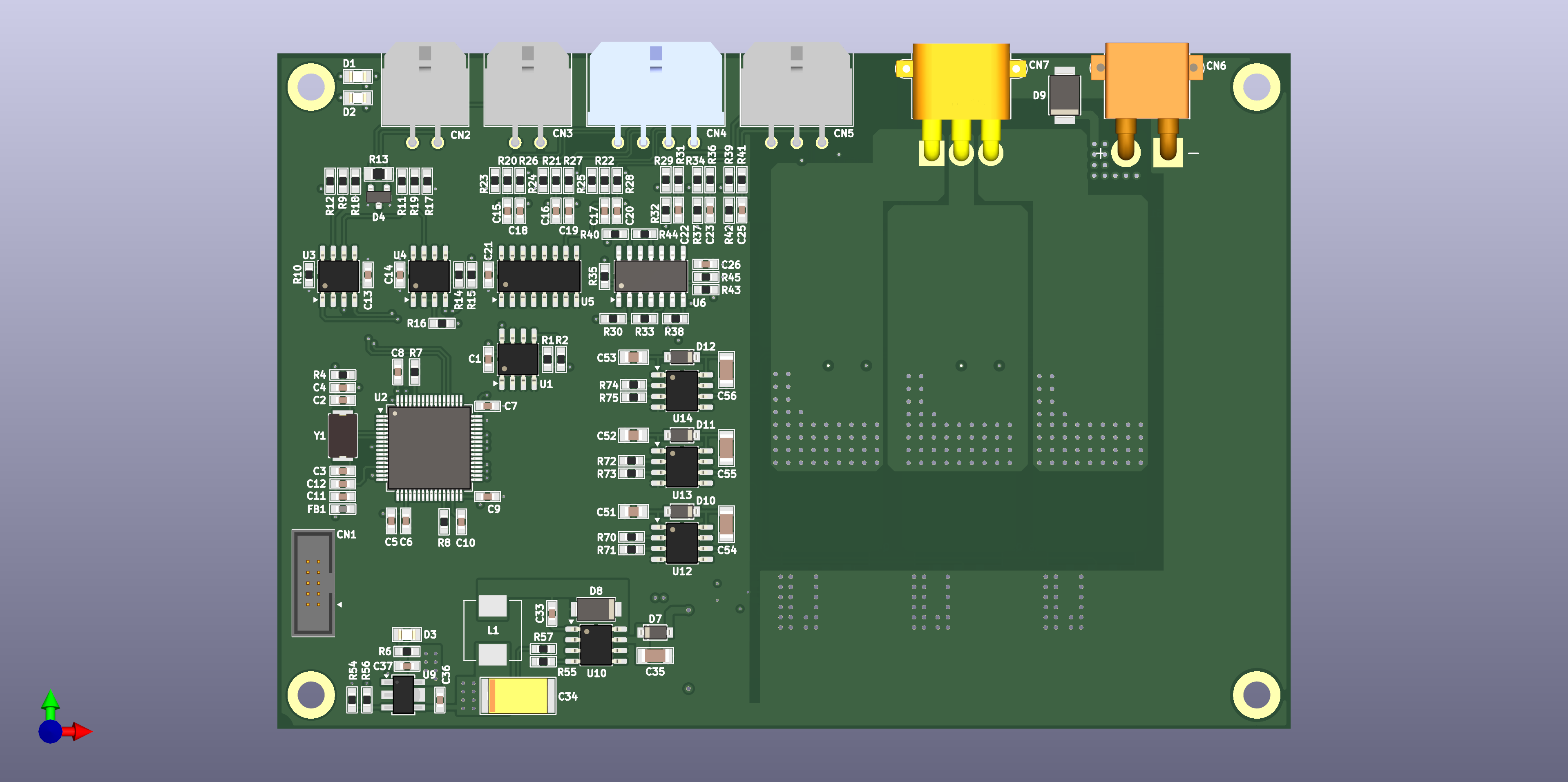
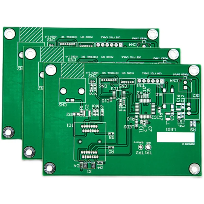
Pcb 회로


![[모집중] PCB 회로설계 및 제작 교육 (ICT디바이스랩 용인)](https://blog.kakaocdn.net/dn/czpU4Q/btrM8g2t3cD/Kz0HHixX50oq7kIErly4q1/img.jpg)


![[직무 길라잡이] PCB 회로설계 직무 (아날로그 회로설계) - YouTube](https://i.ytimg.com/vi/L-bRQRL1xeg/maxresdefault.jpg)


![[e돋보기] PCB(인쇄회로기판)](https://img-lb.inews24.com/image_gisa/201511/1446868148506_1_124959.jpg)


![[3D CAD] 전자 회로기판 PCB설계를 위한 용어정리_[Printed Circuit Board] - 네이버 TV](https://phinf.pstatic.net/tvcast/20191127_284/cHS2U_1574837100452K9cE3_JPEG/1c16be70-10e1-11ea-9d15-505dac8c3607_02.jpg?type=f1109_624)


Advance healthcare with our stunning medical Pcb 회로 collection of comprehensive galleries of clinical images. medically documenting photography, images, and pictures. designed to support medical professionals. Browse our premium Pcb 회로 gallery featuring professionally curated photographs. Suitable for various applications including web design, social media, personal projects, and digital content creation All Pcb 회로 images are available in high resolution with professional-grade quality, optimized for both digital and print applications, and include comprehensive metadata for easy organization and usage. Discover the perfect Pcb 회로 images to enhance your visual communication needs. Comprehensive tagging systems facilitate quick discovery of relevant Pcb 회로 content. The Pcb 회로 collection represents years of careful curation and professional standards. The Pcb 회로 archive serves professionals, educators, and creatives across diverse industries. Whether for commercial projects or personal use, our Pcb 회로 collection delivers consistent excellence. Multiple resolution options ensure optimal performance across different platforms and applications. Cost-effective licensing makes professional Pcb 회로 photography accessible to all budgets. Reliable customer support ensures smooth experience throughout the Pcb 회로 selection process. Regular updates keep the Pcb 회로 collection current with contemporary trends and styles. Instant download capabilities enable immediate access to chosen Pcb 회로 images. Each image in our Pcb 회로 gallery undergoes rigorous quality assessment before inclusion. Our Pcb 회로 database continuously expands with fresh, relevant content from skilled photographers.