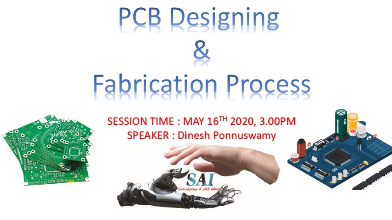
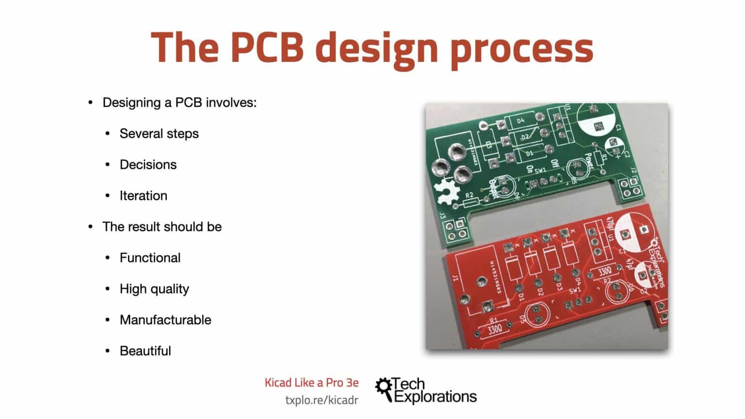
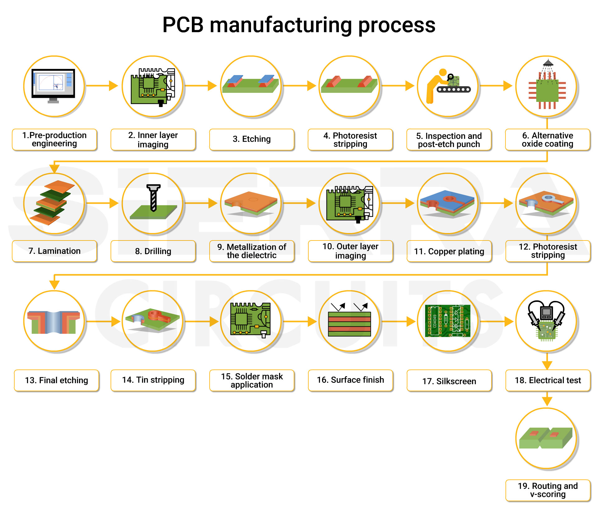
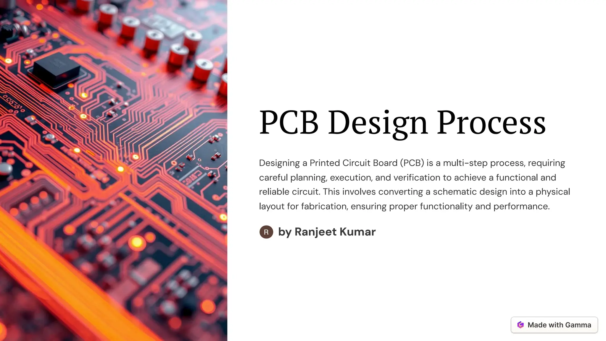
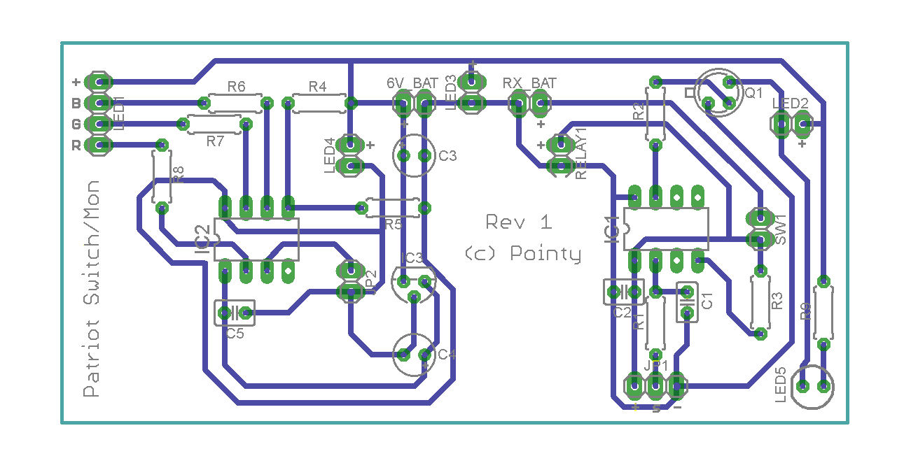
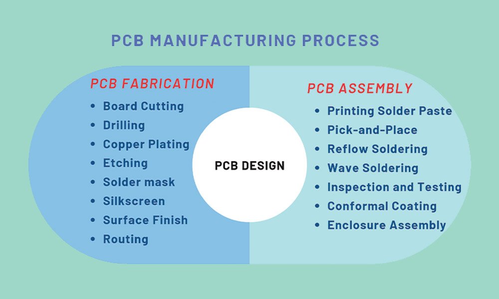
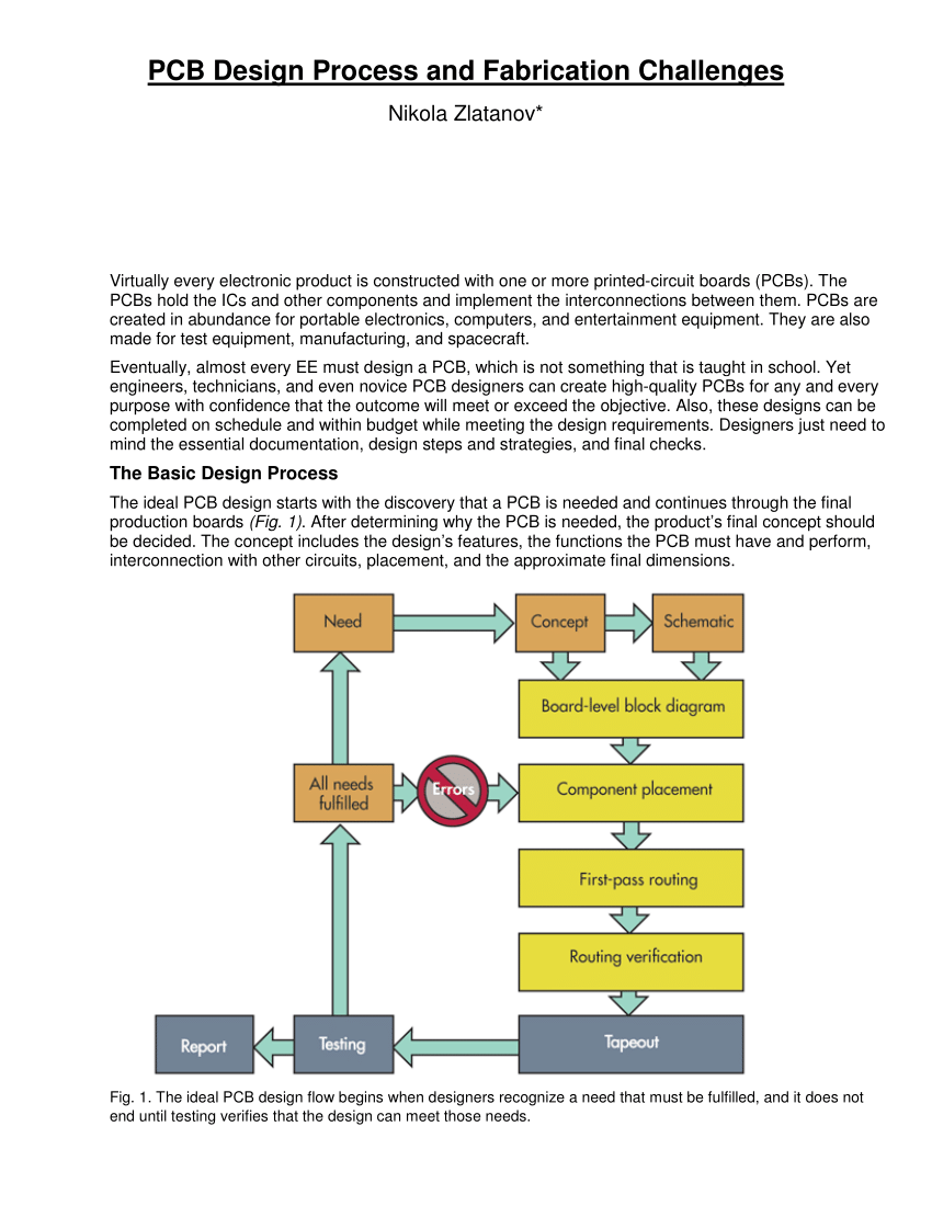
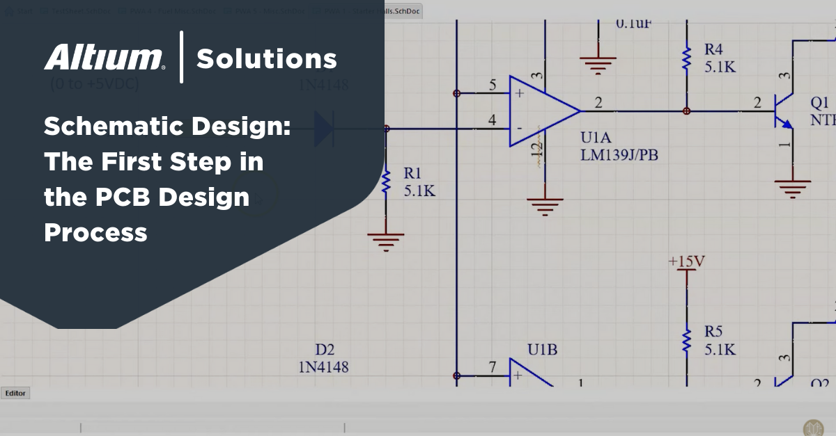
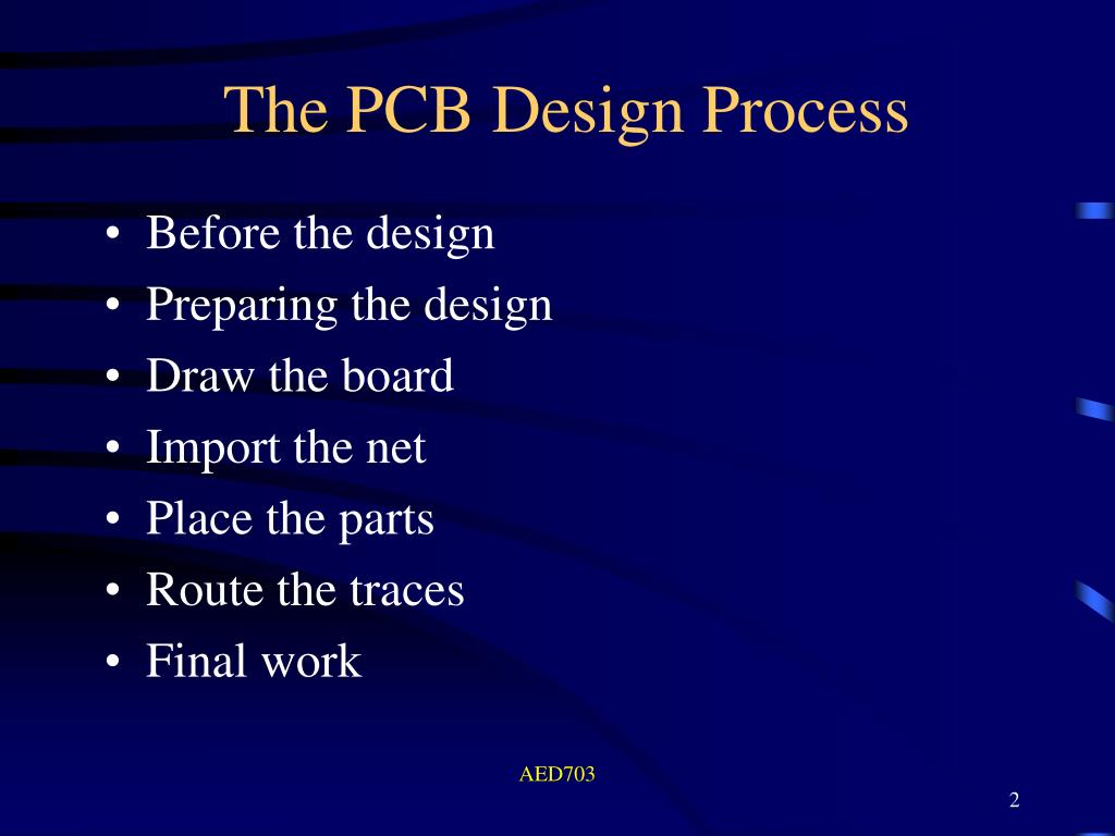
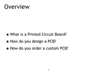
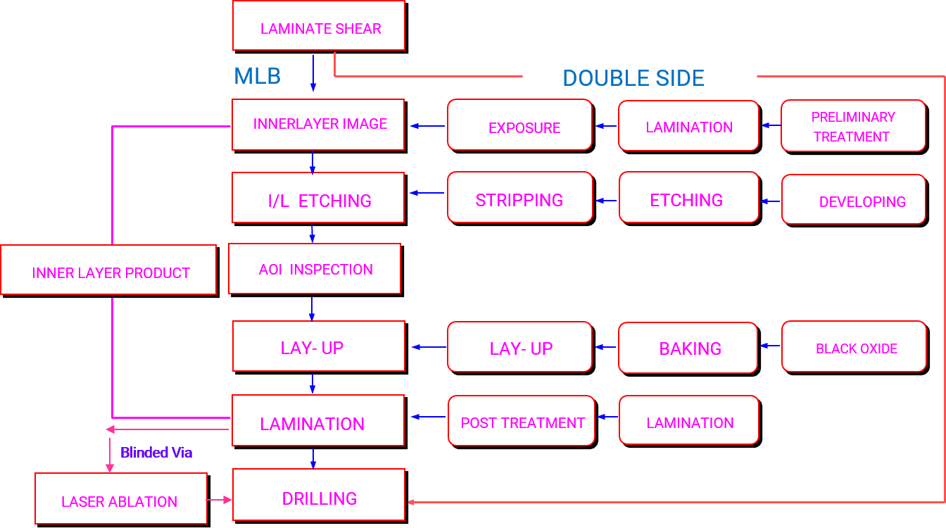
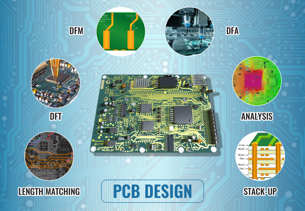
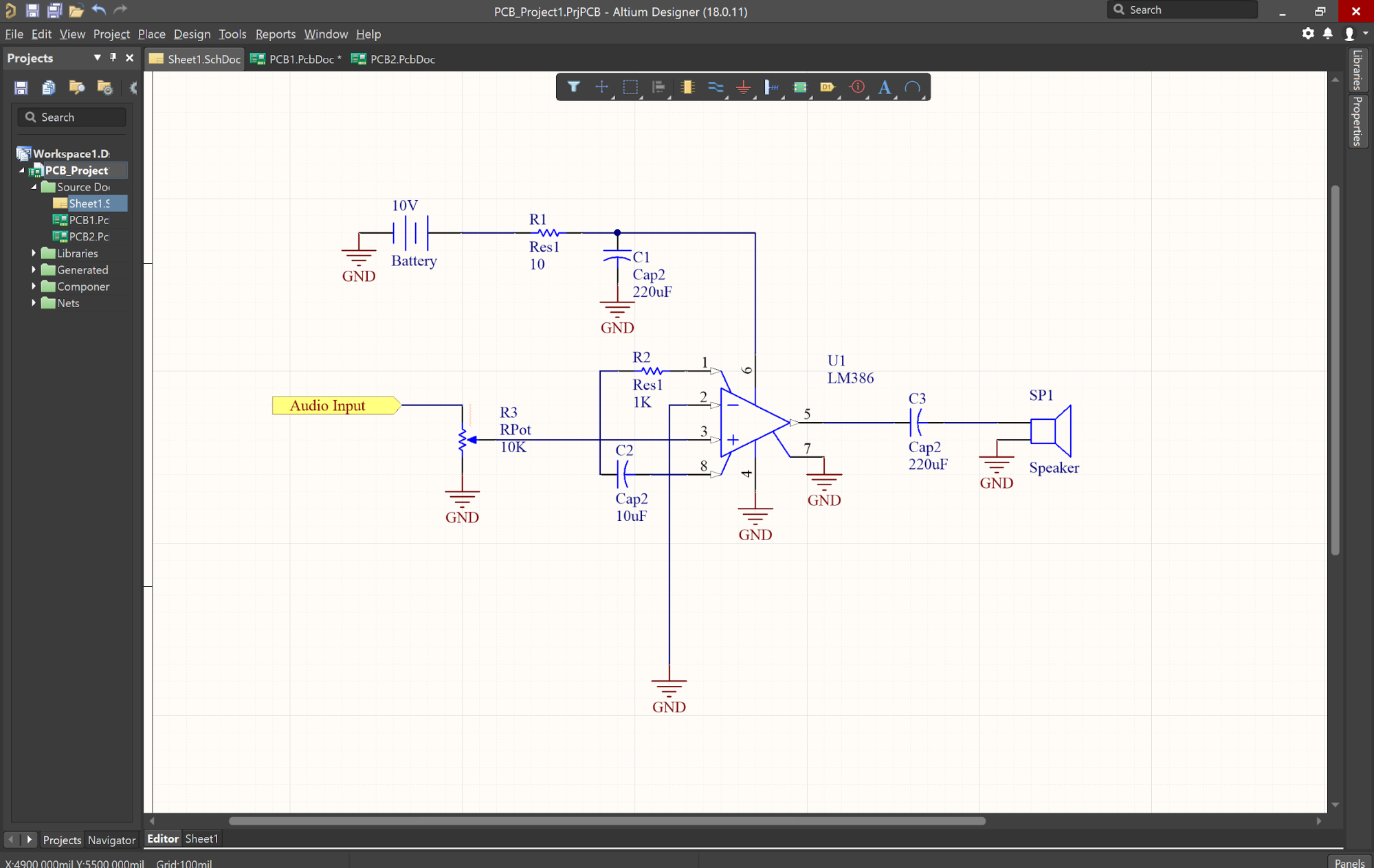
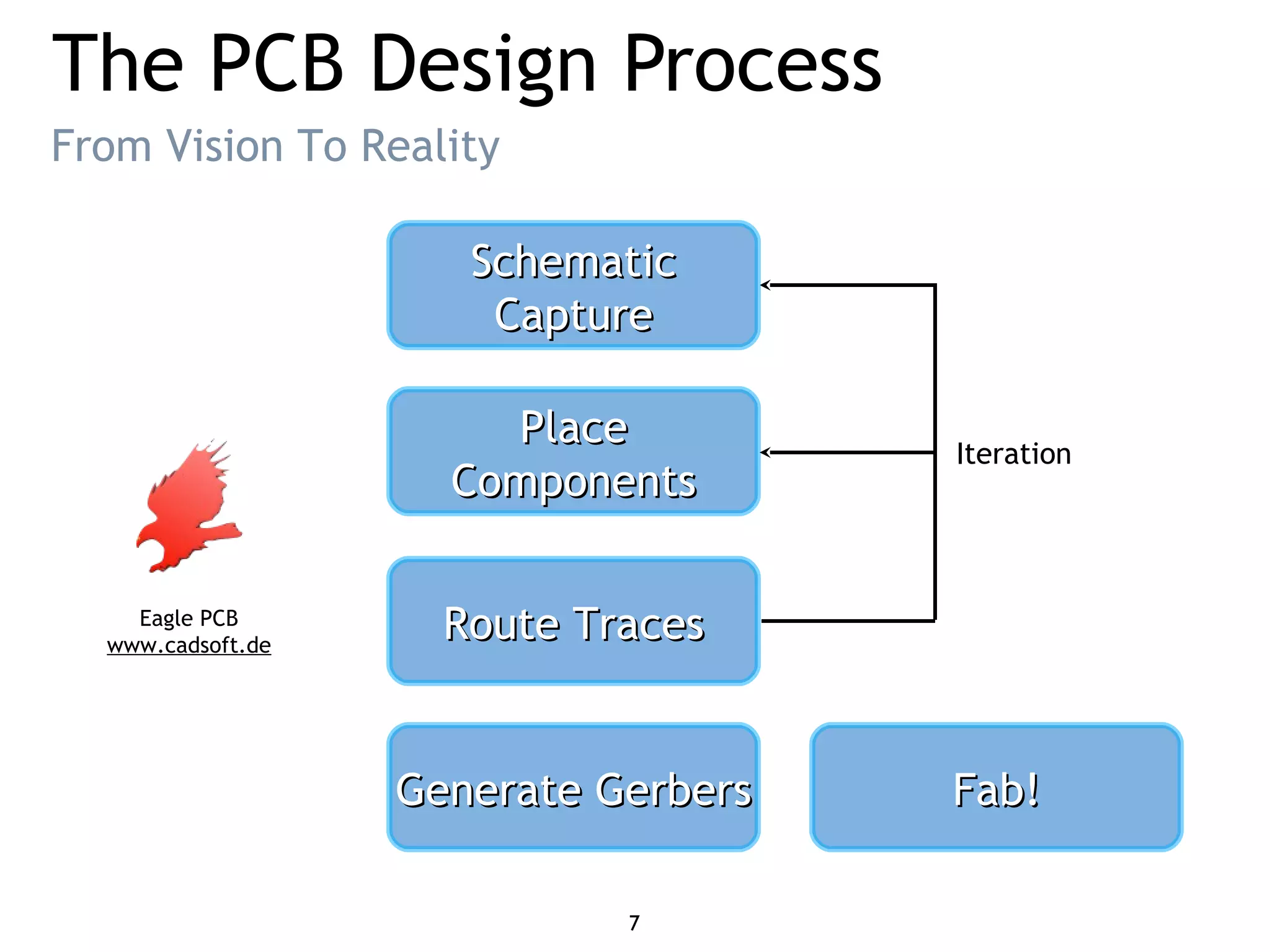
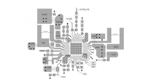
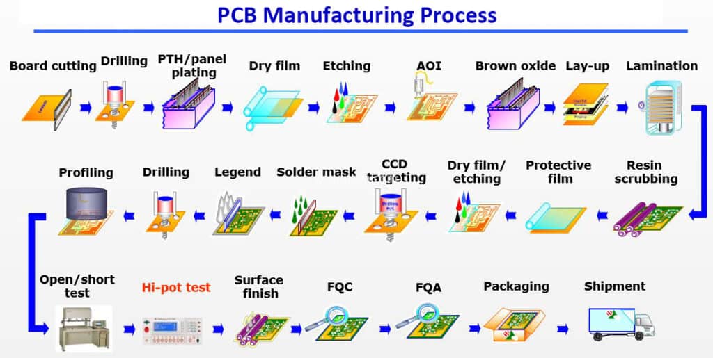
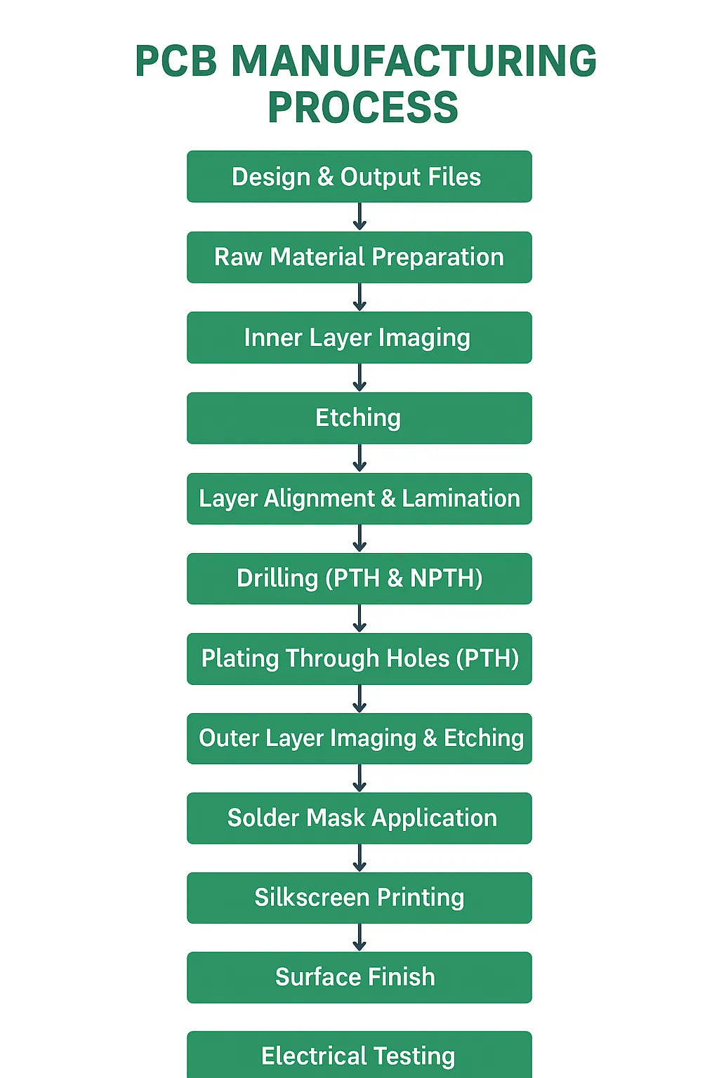
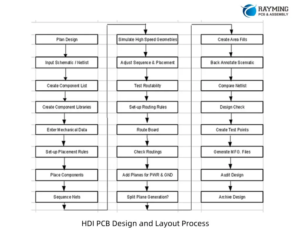
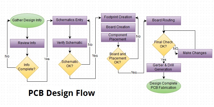
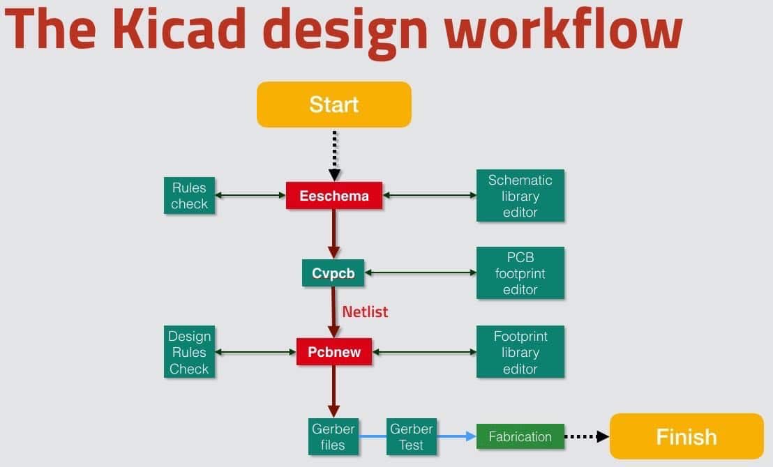
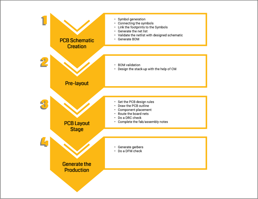
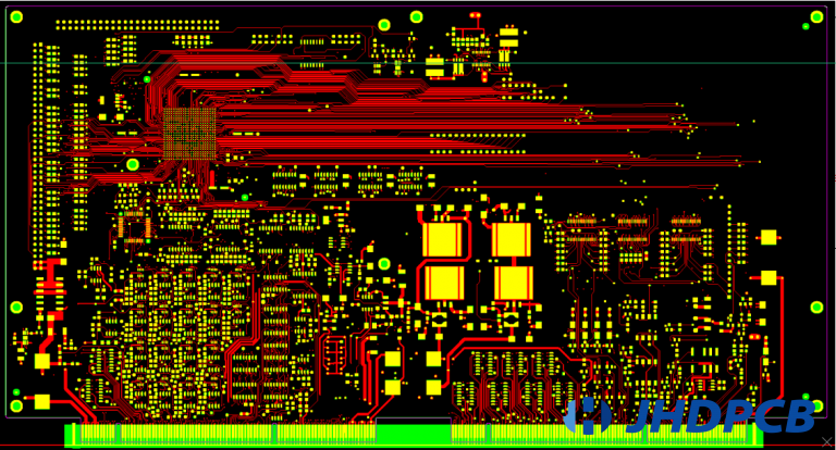
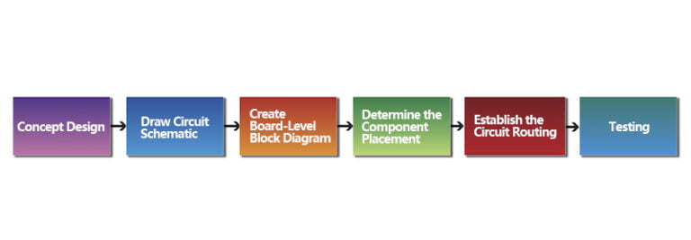
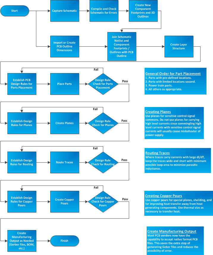
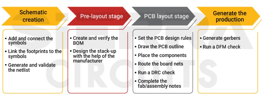
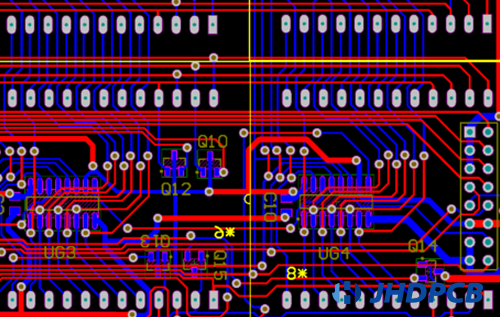
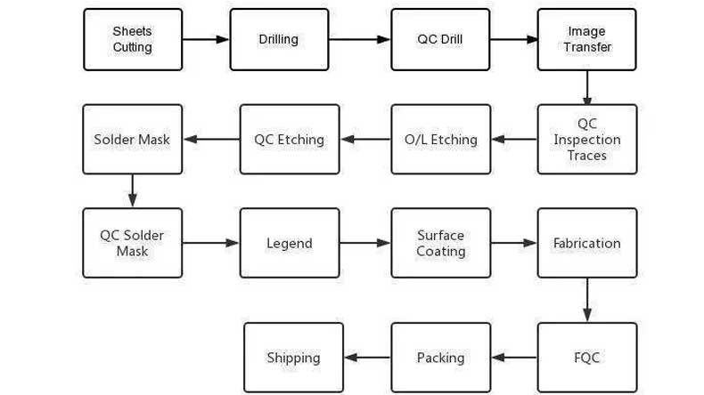
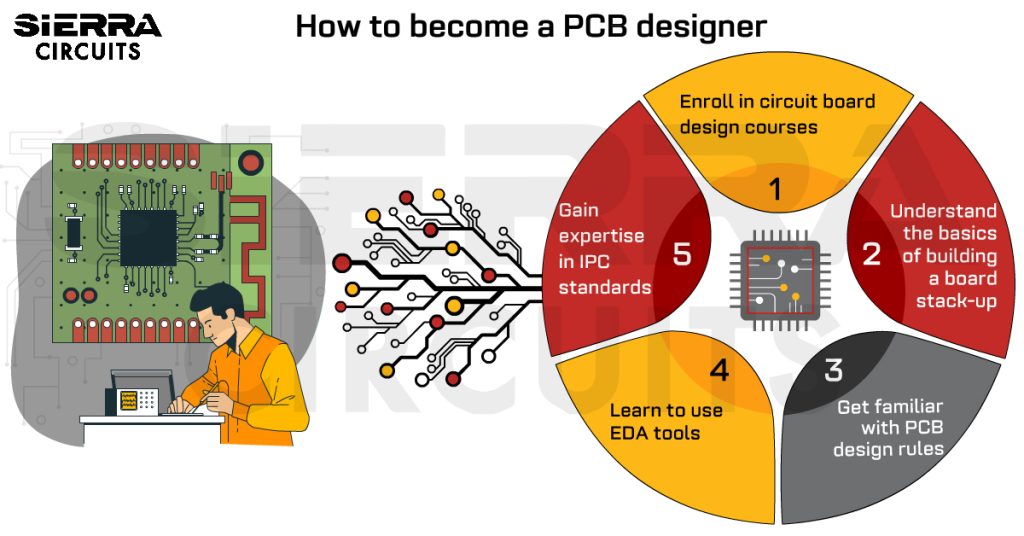
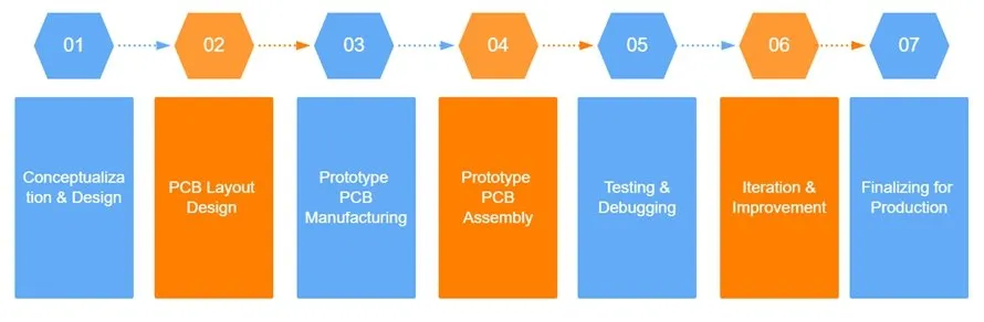
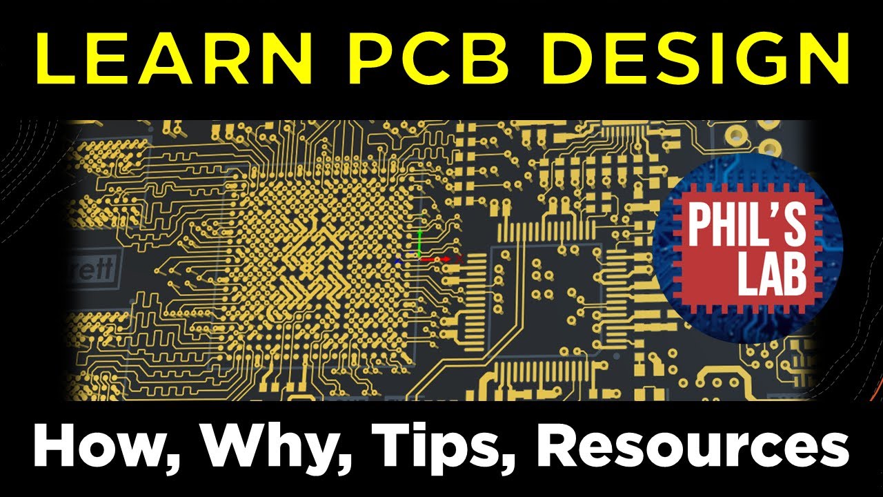
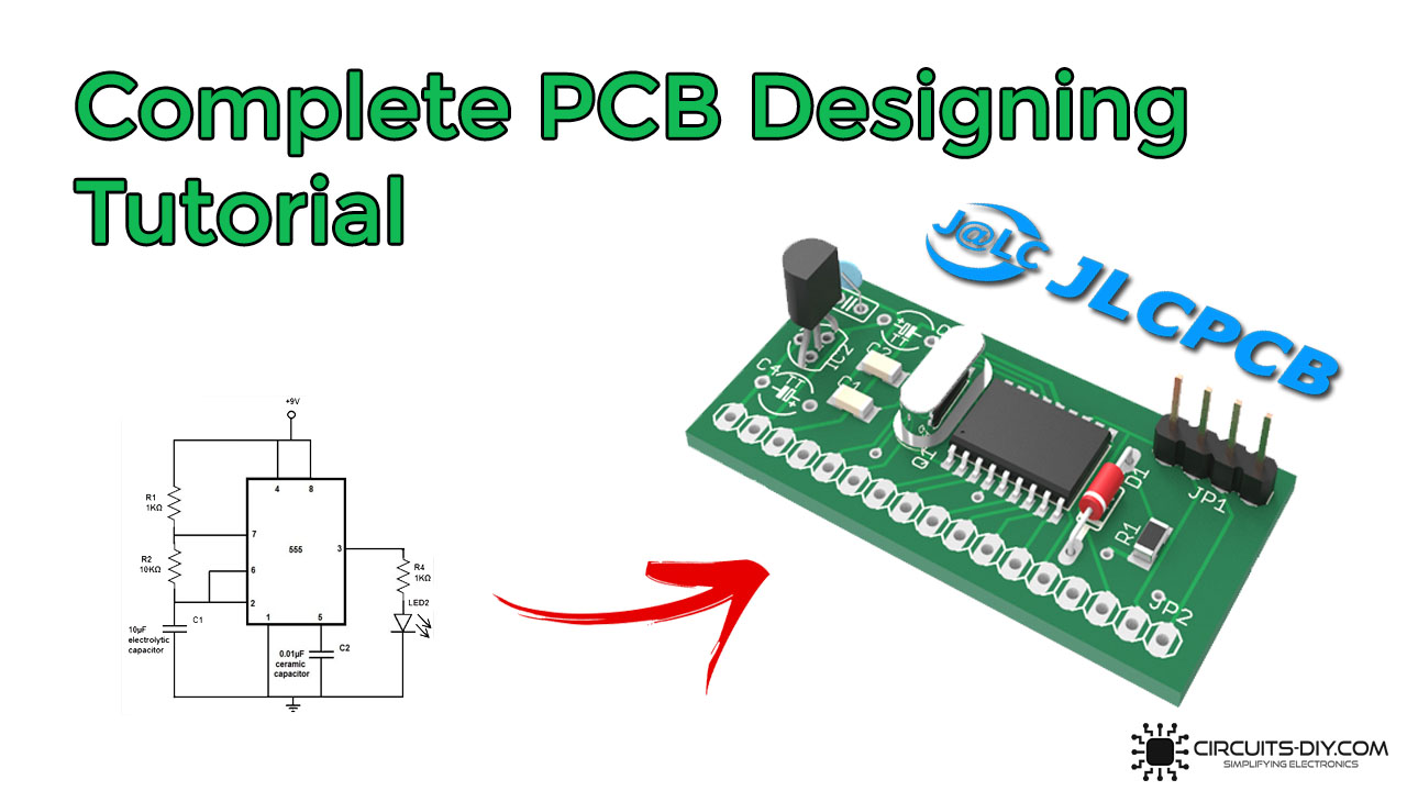
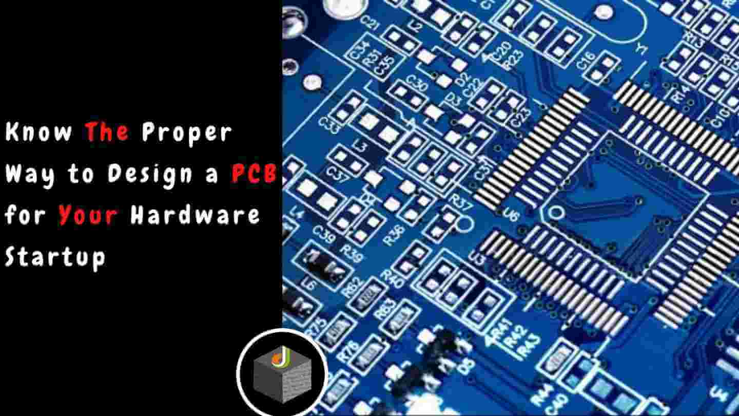
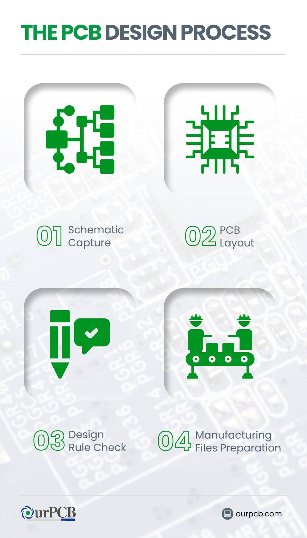
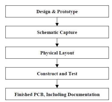
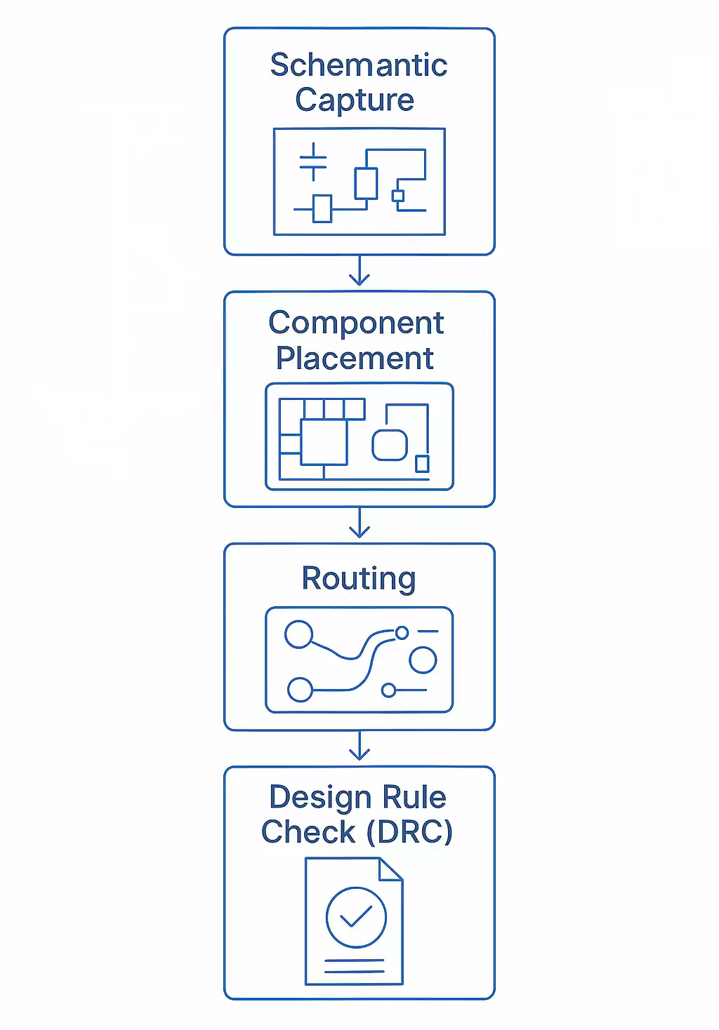
Pcb Designing Process


![PCB Designing ,Layout and Assembly basics For Beginners [2022]](https://www.electronicsandyou.com/blog/wp-content/uploads/2019/03/multilayer-pcb.jpg)


.png)
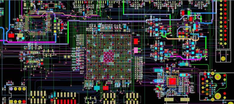


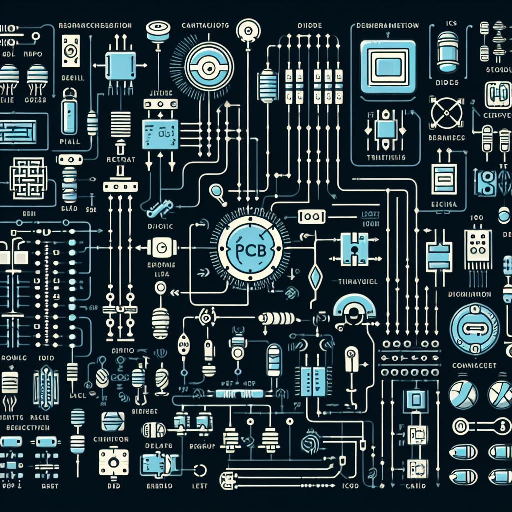


Experience the pulse of Pcb Designing Process with our extensive urban gallery of extensive collections of images. showcasing the architectural beauty of artistic, creative, and design. ideal for architectural and street photography. Our Pcb Designing Process collection features high-quality images with excellent detail and clarity. Suitable for various applications including web design, social media, personal projects, and digital content creation All Pcb Designing Process images are available in high resolution with professional-grade quality, optimized for both digital and print applications, and include comprehensive metadata for easy organization and usage. Discover the perfect Pcb Designing Process images to enhance your visual communication needs. Regular updates keep the Pcb Designing Process collection current with contemporary trends and styles. Reliable customer support ensures smooth experience throughout the Pcb Designing Process selection process. Instant download capabilities enable immediate access to chosen Pcb Designing Process images. Multiple resolution options ensure optimal performance across different platforms and applications. Our Pcb Designing Process database continuously expands with fresh, relevant content from skilled photographers. Advanced search capabilities make finding the perfect Pcb Designing Process image effortless and efficient. Cost-effective licensing makes professional Pcb Designing Process photography accessible to all budgets. The Pcb Designing Process archive serves professionals, educators, and creatives across diverse industries.