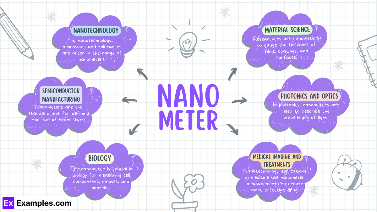
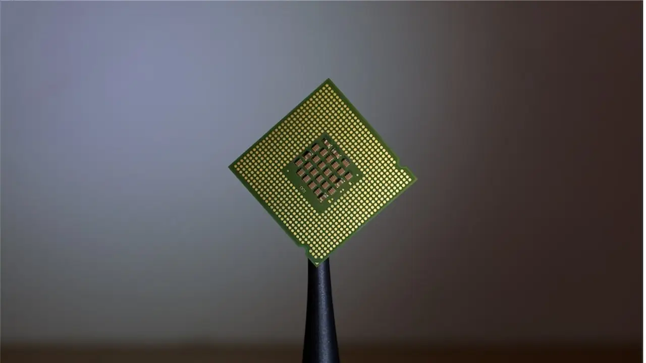
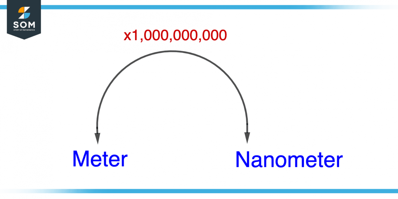
Nanometer Process


![[News] The Imminent Arrival of 2-Nanometer Advanced Process](https://img.trendforce.com/blog/wp-content/uploads/2023/09/20113557/%E6%99%B6%E5%9C%93%E4%BB%A3%E5%B7%A5%E5%BB%A0%E5%85%88%E9%80%B2%E8%A3%BD%E7%A8%8B%E8%B7%AF%E7%B7%9A%E5%9C%96_ENG.png)
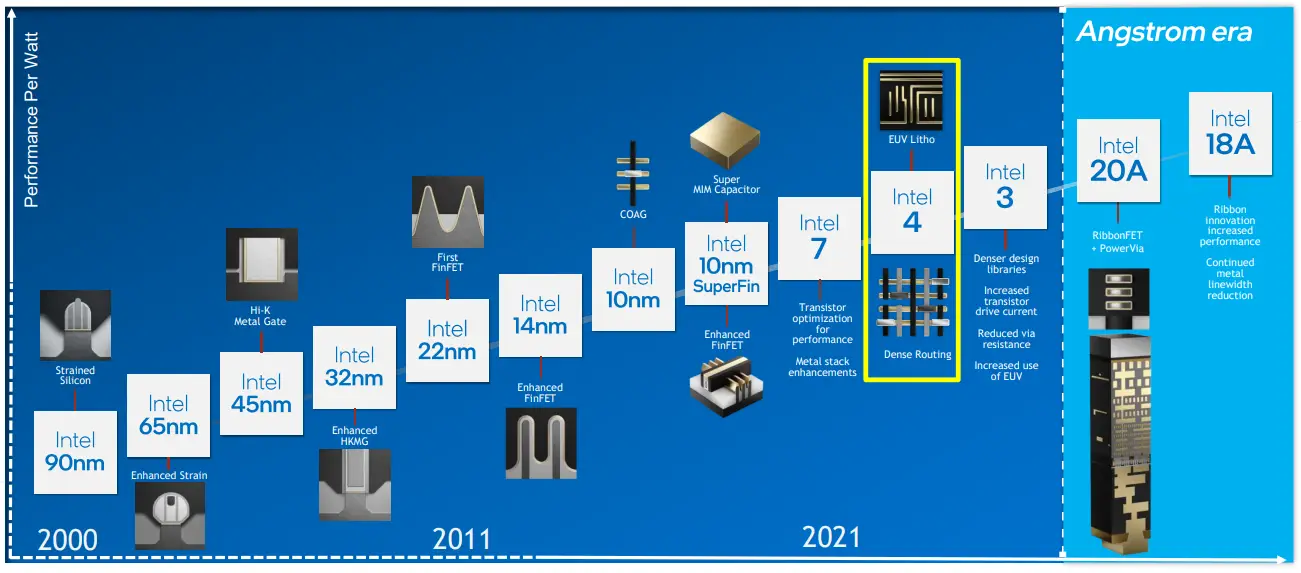


![[News] Intel Promotes 1.8-Nanometer Process in South Korea, Reportedly ...](https://img.trendforce.com/blog/wp-content/uploads/2024/02/22140505/intel-foundry-node-roadmap-2024.png.rendition.intel_.web_.1648.927.png)
:quality(90)/p7i.vogel.de/wcms/d7/df/d7df3b9c96eae82b5f0261f0b02eeaed/0123923136v1.jpeg)


![[News] The Intense Battle of 2-Nanometer Technology Set to Escalate ...](https://img.trendforce.com/blog/wp-content/uploads/2024/03/27152638/1711524321924.jpg)


![[News] Advancing into Intel 10A! Intel’s 2027 Blueprint Adds 1 ...](https://img.trendforce.com/blog/wp-content/uploads/2024/02/22153607/Intel-Foundry-IFDC-2-1024x683.jpg)


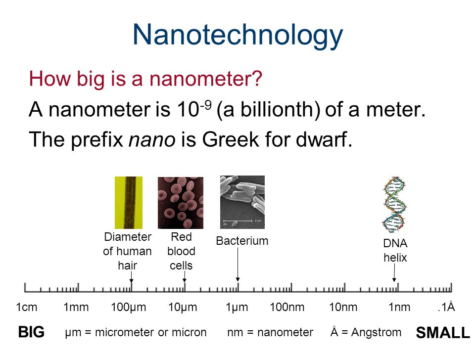
Facilitate learning with our scientific Nanometer Process gallery of vast arrays of educational images. scientifically documenting photography, images, and pictures. perfect for research publications and studies. The Nanometer Process collection maintains consistent quality standards across all images. Suitable for various applications including web design, social media, personal projects, and digital content creation All Nanometer Process images are available in high resolution with professional-grade quality, optimized for both digital and print applications, and include comprehensive metadata for easy organization and usage. Our Nanometer Process gallery offers diverse visual resources to bring your ideas to life. Cost-effective licensing makes professional Nanometer Process photography accessible to all budgets. Our Nanometer Process database continuously expands with fresh, relevant content from skilled photographers. The Nanometer Process archive serves professionals, educators, and creatives across diverse industries. Professional licensing options accommodate both commercial and educational usage requirements. Comprehensive tagging systems facilitate quick discovery of relevant Nanometer Process content. Time-saving browsing features help users locate ideal Nanometer Process images quickly. Regular updates keep the Nanometer Process collection current with contemporary trends and styles. Diverse style options within the Nanometer Process collection suit various aesthetic preferences. The Nanometer Process collection represents years of careful curation and professional standards. Whether for commercial projects or personal use, our Nanometer Process collection delivers consistent excellence.