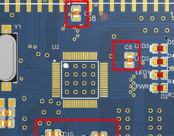
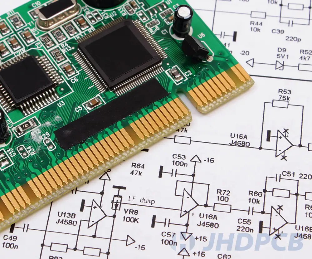
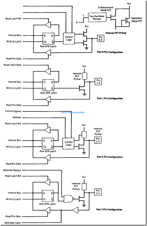
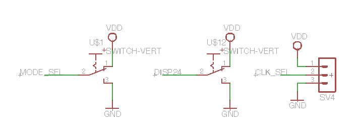
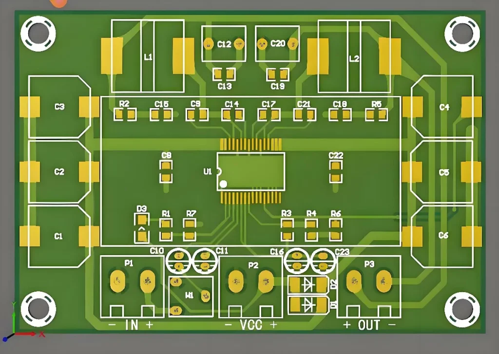
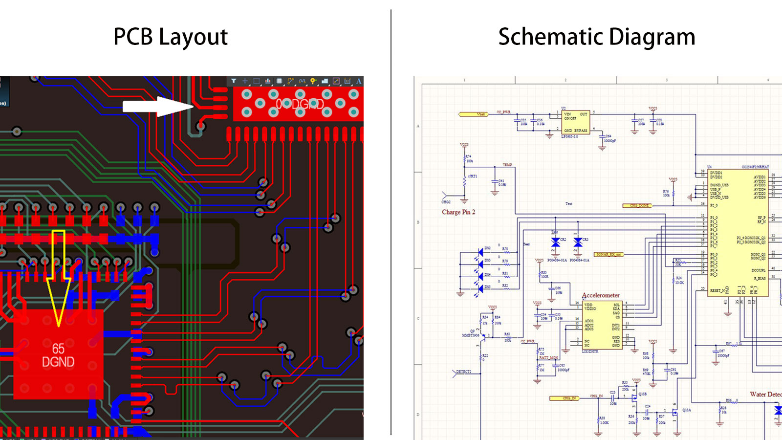
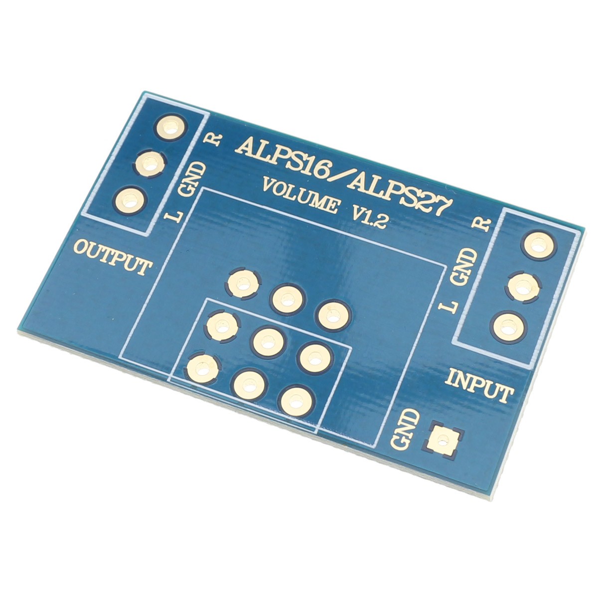
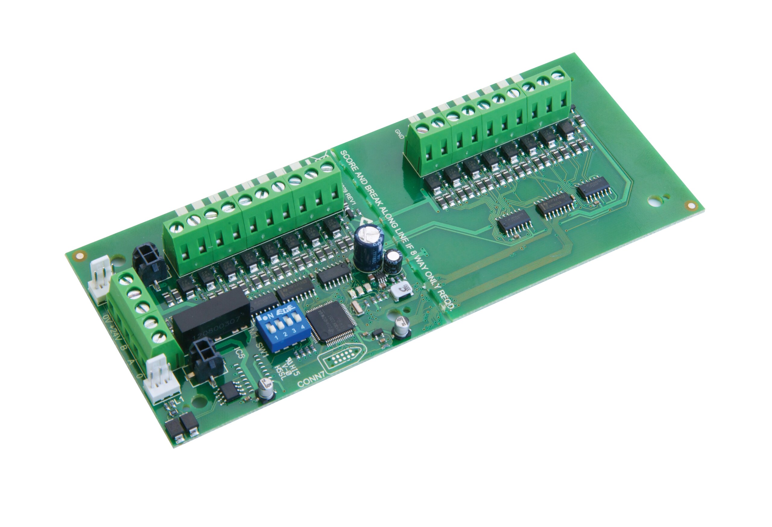
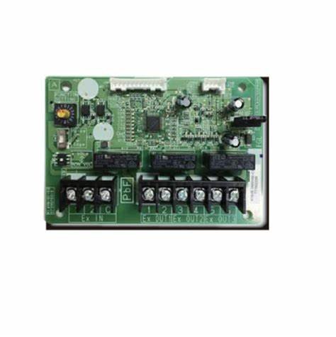
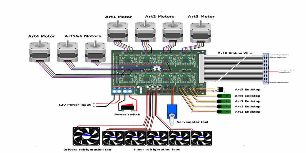
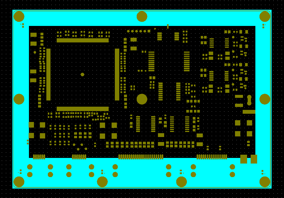
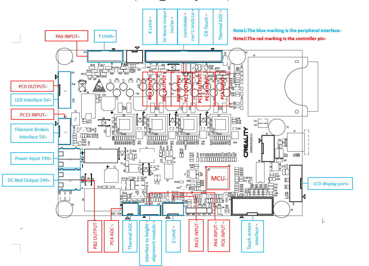
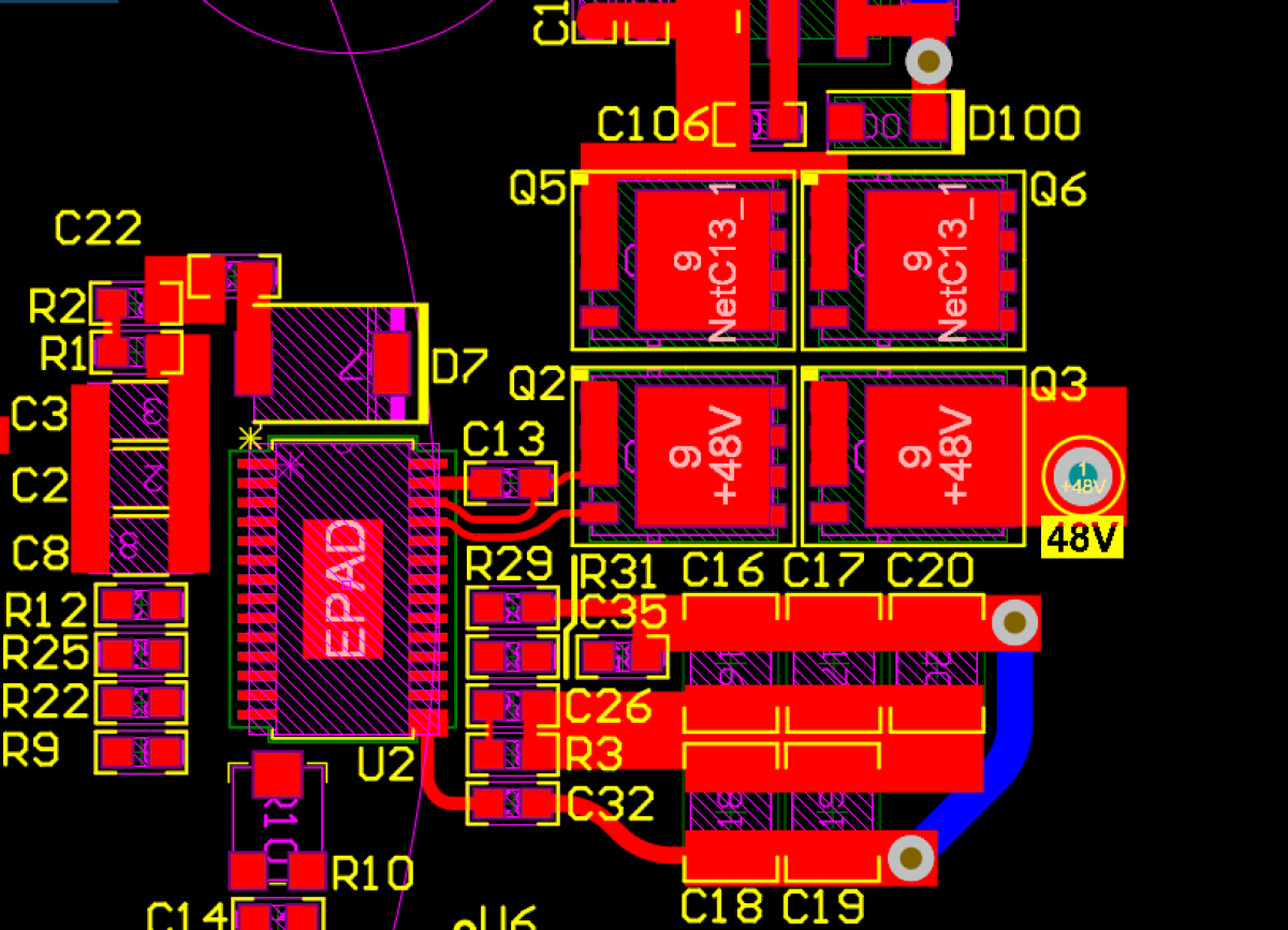
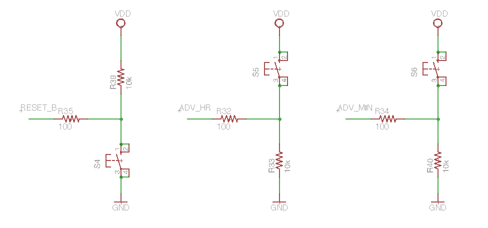
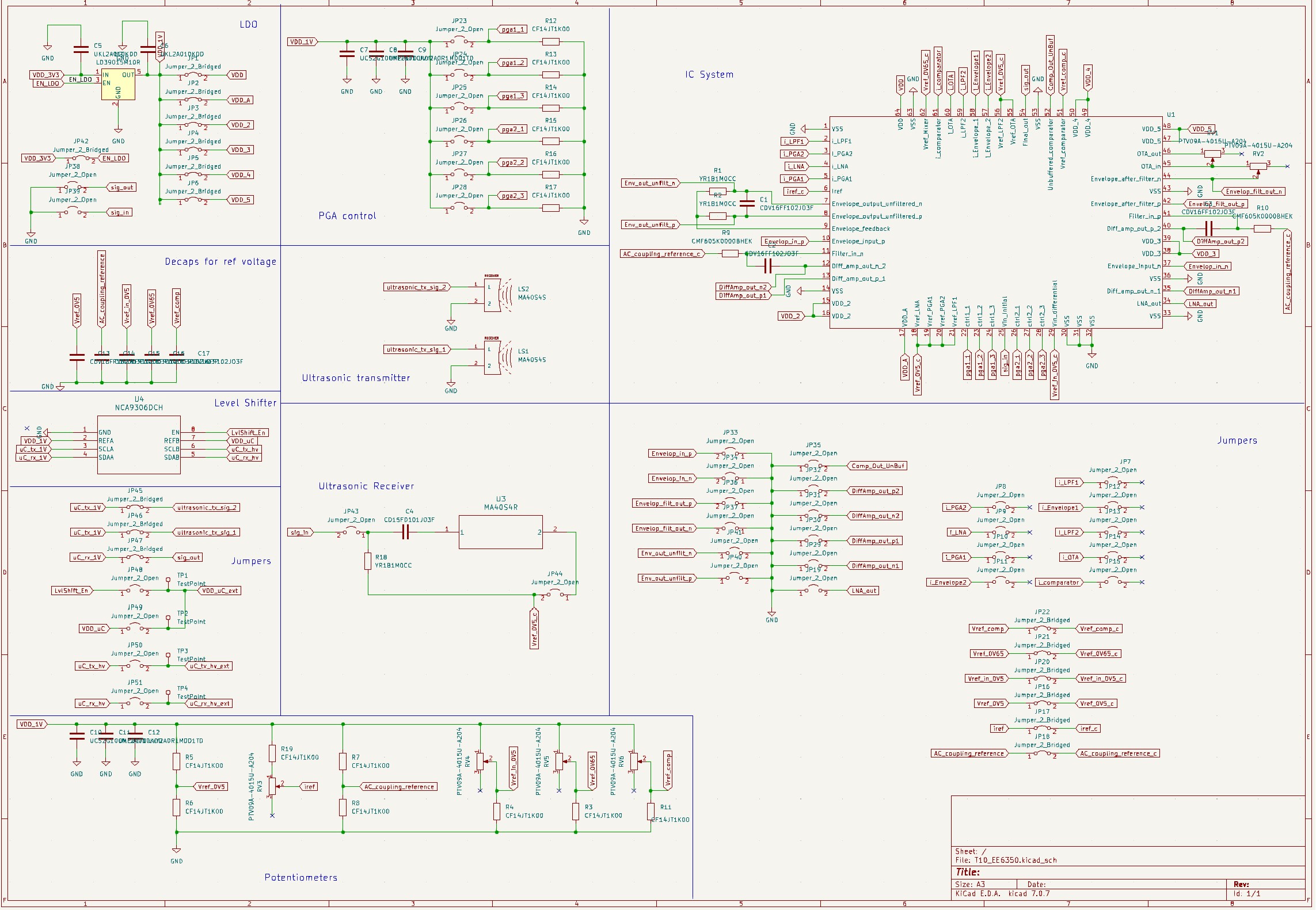
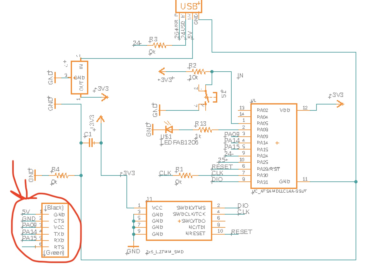
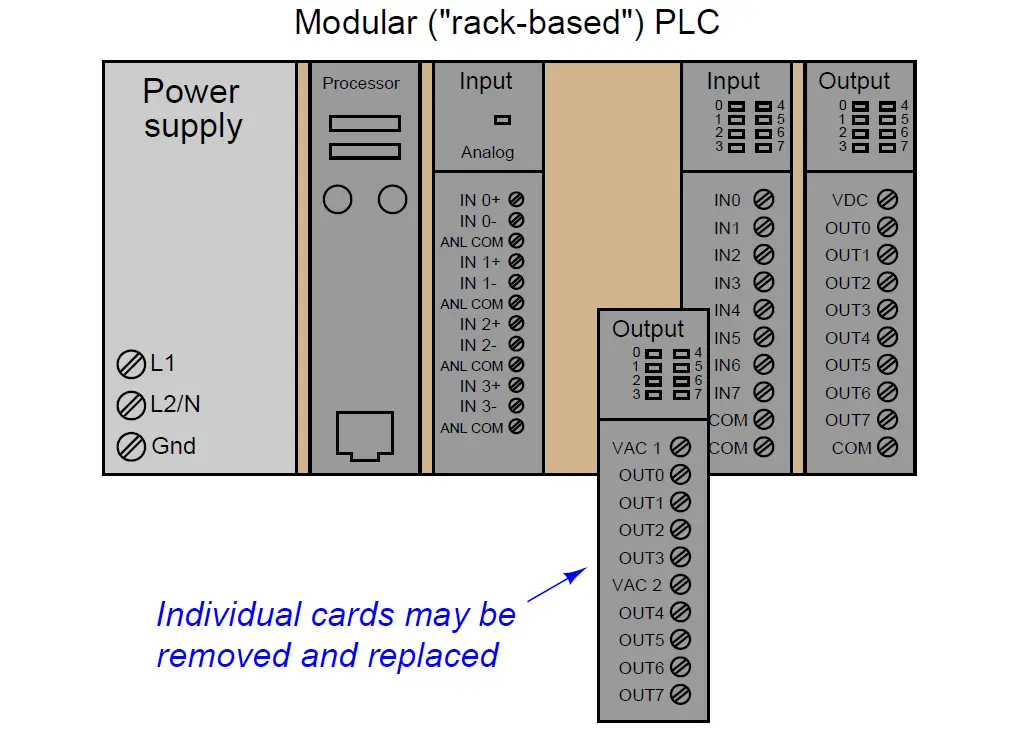
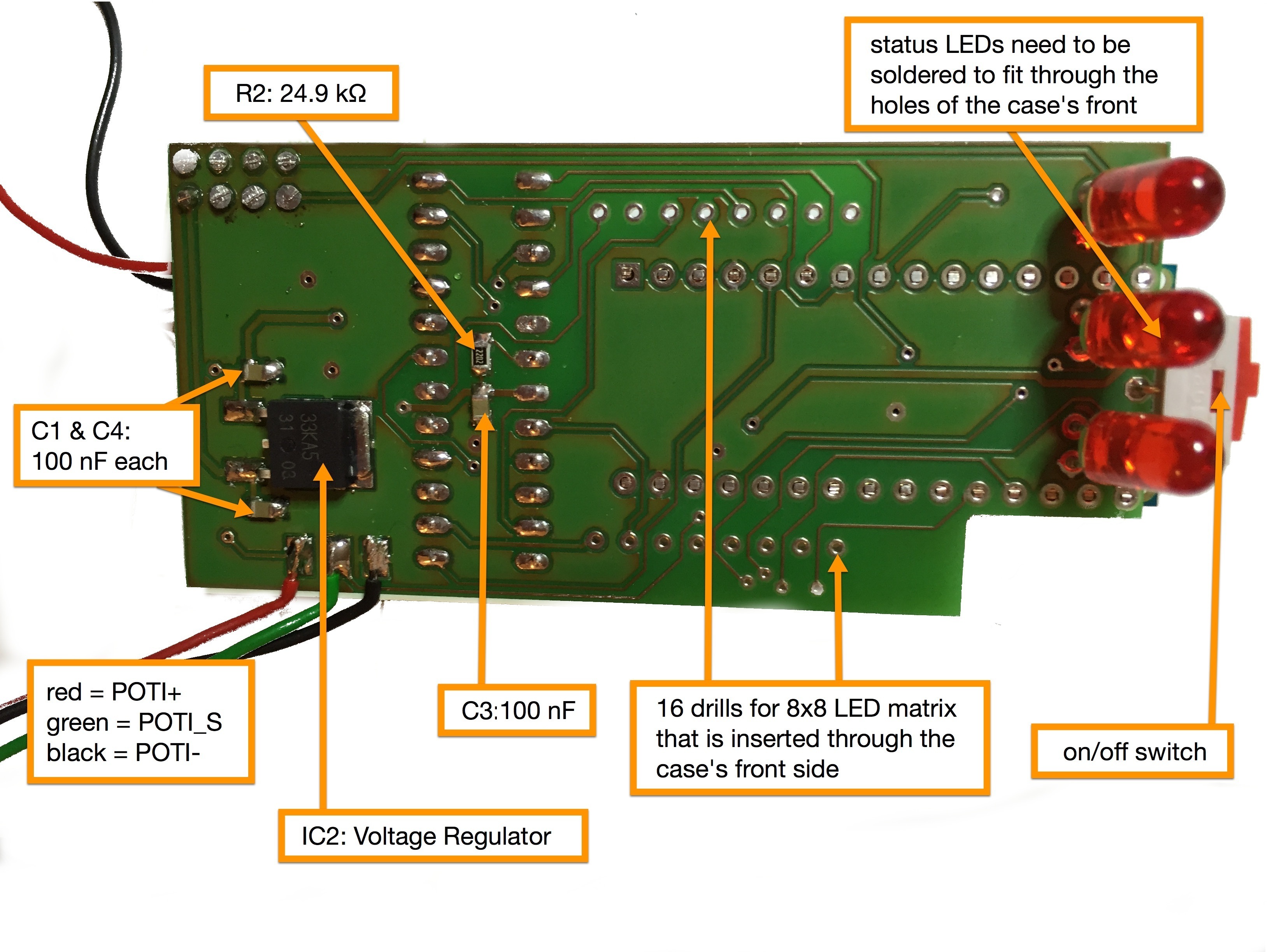
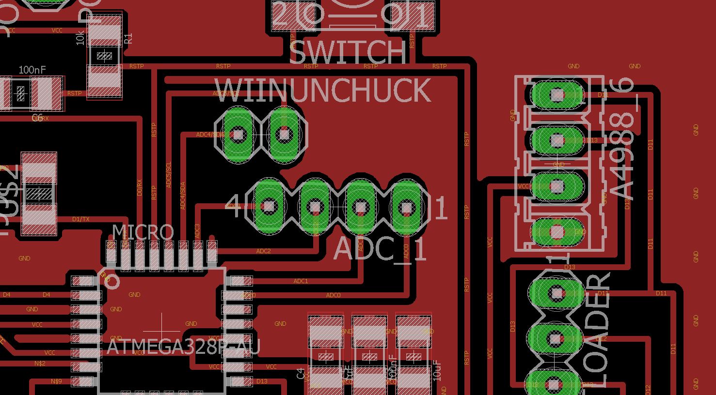
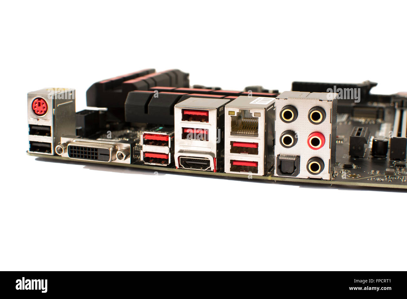
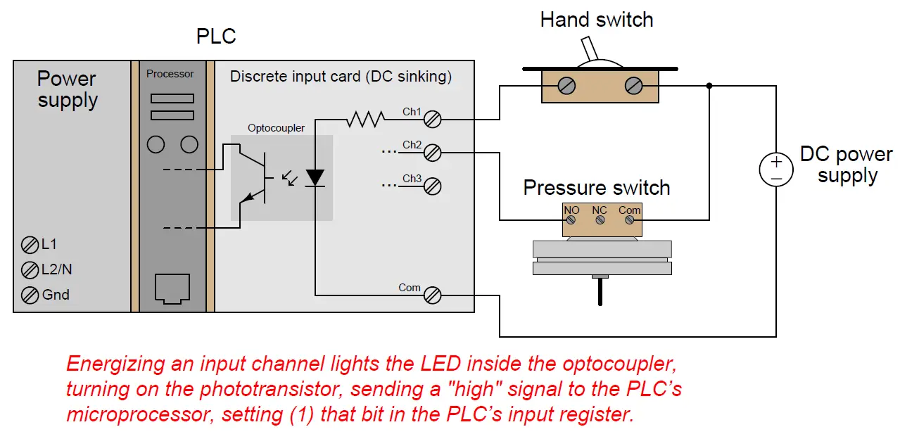
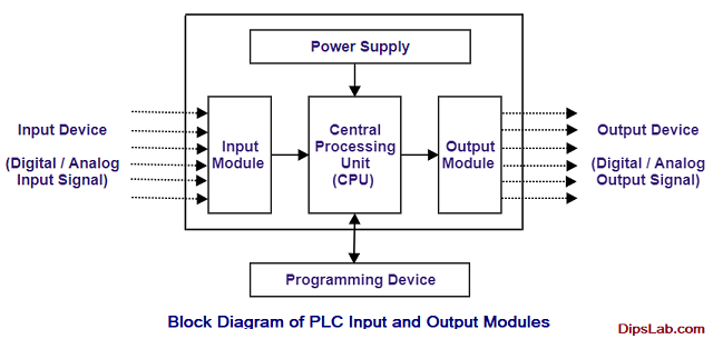
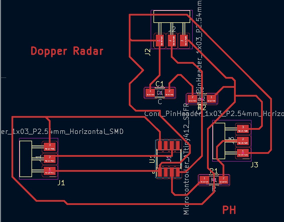
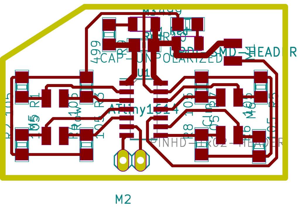
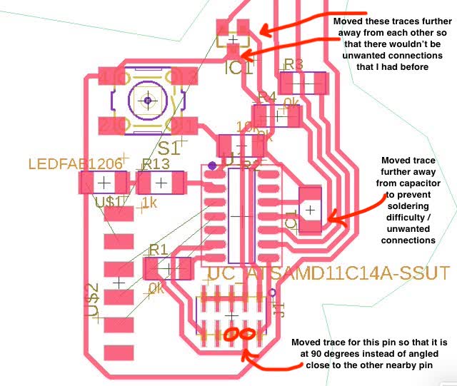
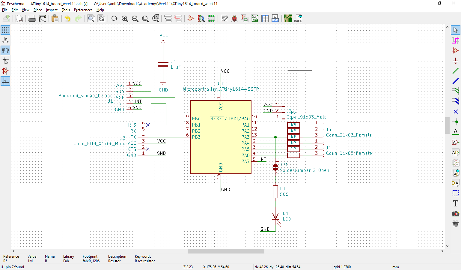
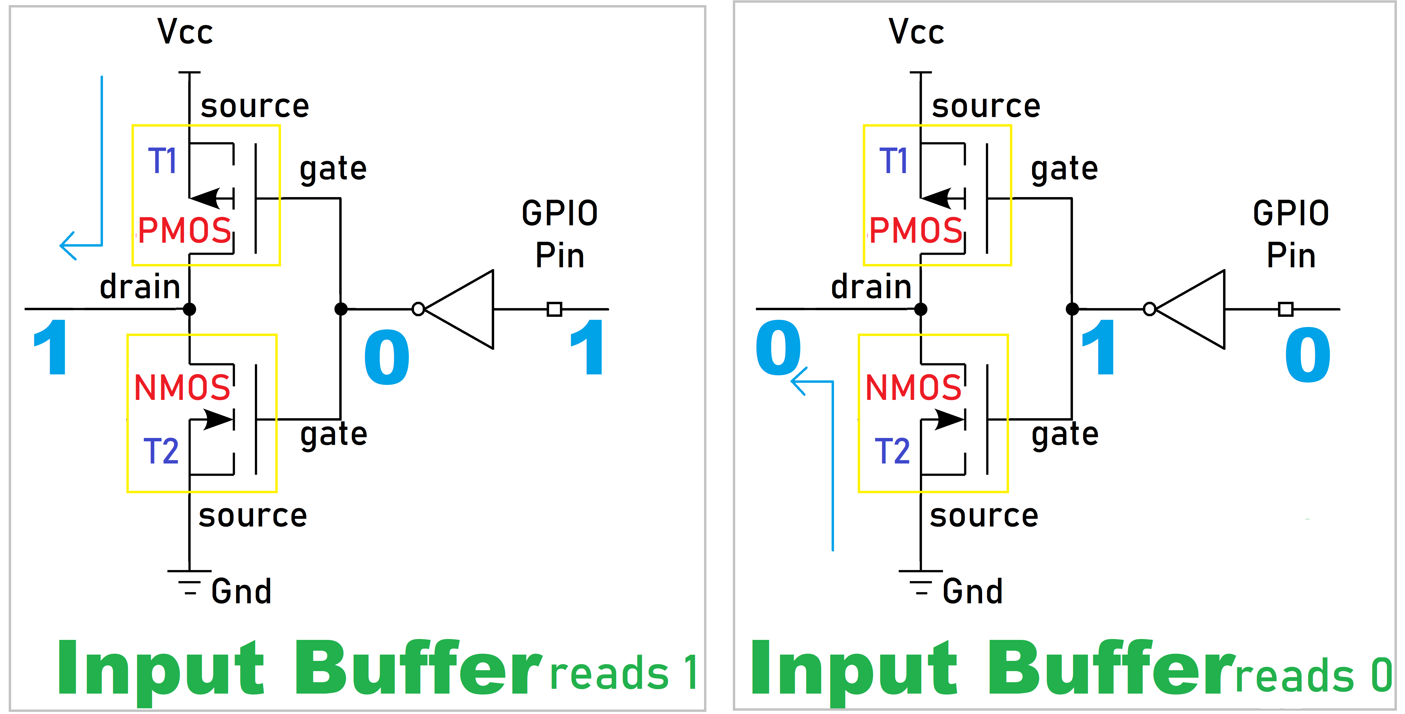
Input/output Location In Pcb


![Fuji Electric FRN22VG1S-2J [139/1046] Figure 3 18 shows the location of ...](https://mcgrp.ru/views2/1575084/page139/bg8b.png)


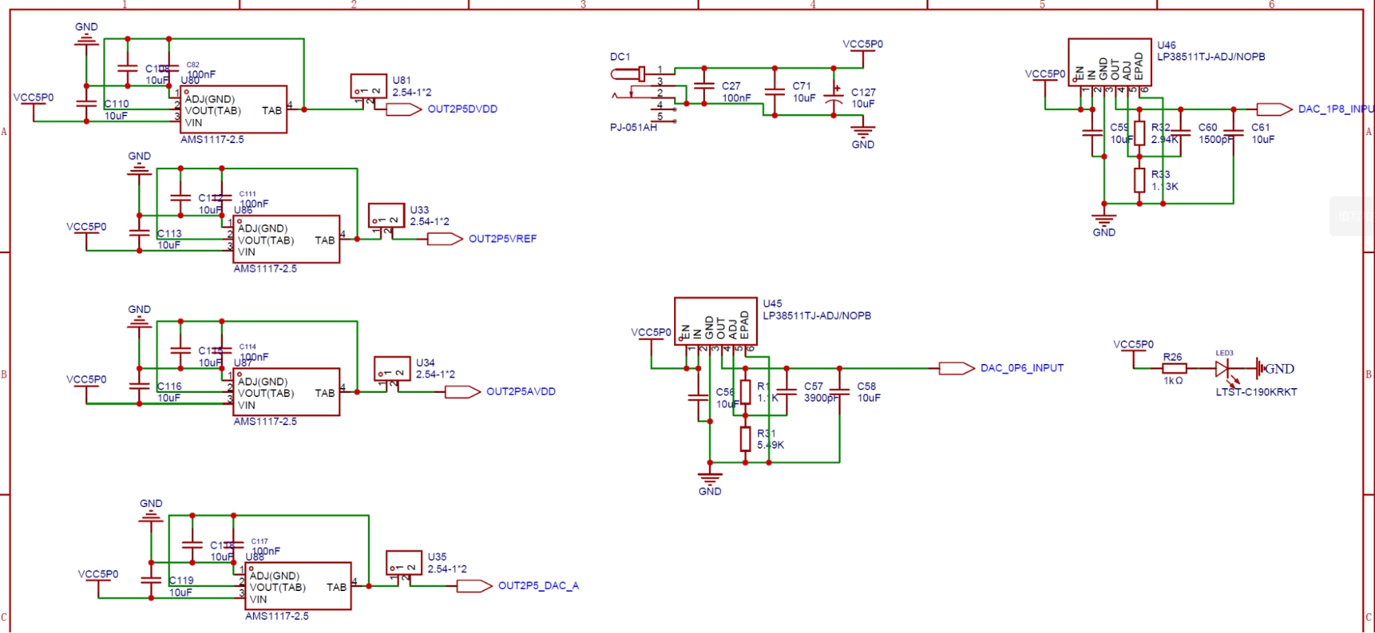
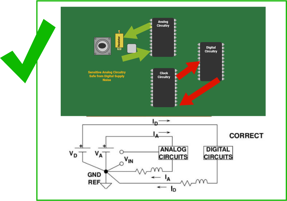
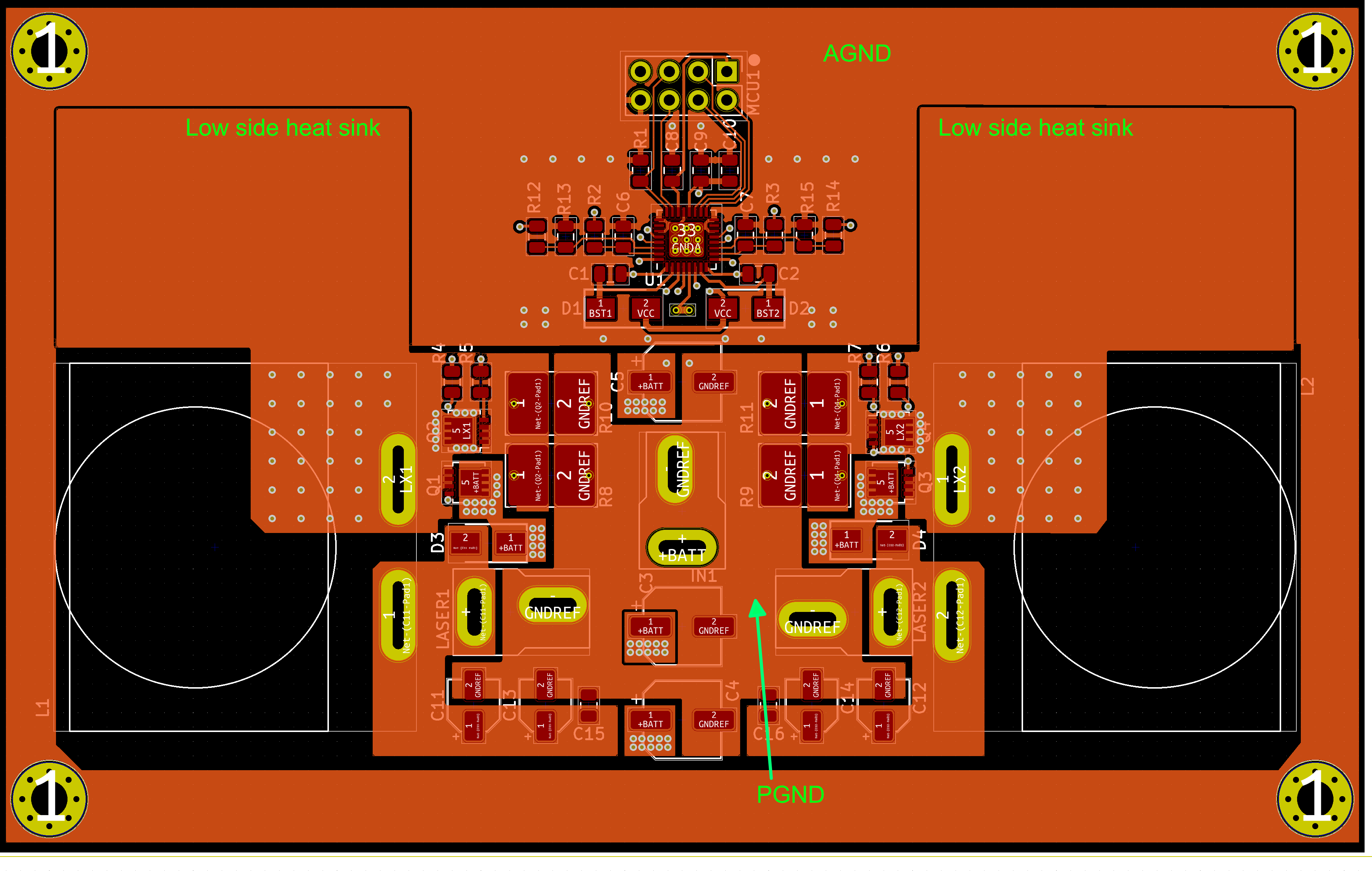
![[PDF] Intro to PCB Design: A Beginner’s Guide to Mastering PCB Layout ...](https://www.raypcb.com/wp-content/uploads/2023/02/PCB-Design-Guidelines-For-EMI-EMC.jpg)


Experience the clarity of Input/output Location In Pcb with our curated collection of substantial collections of images. highlighting the purity of photography, images, and pictures. perfect for modern design and branding. Discover high-resolution Input/output Location In Pcb images optimized for various applications. Suitable for various applications including web design, social media, personal projects, and digital content creation All Input/output Location In Pcb images are available in high resolution with professional-grade quality, optimized for both digital and print applications, and include comprehensive metadata for easy organization and usage. Explore the versatility of our Input/output Location In Pcb collection for various creative and professional projects. The Input/output Location In Pcb collection represents years of careful curation and professional standards. Comprehensive tagging systems facilitate quick discovery of relevant Input/output Location In Pcb content. The Input/output Location In Pcb archive serves professionals, educators, and creatives across diverse industries. Multiple resolution options ensure optimal performance across different platforms and applications. Instant download capabilities enable immediate access to chosen Input/output Location In Pcb images. Diverse style options within the Input/output Location In Pcb collection suit various aesthetic preferences. Each image in our Input/output Location In Pcb gallery undergoes rigorous quality assessment before inclusion.