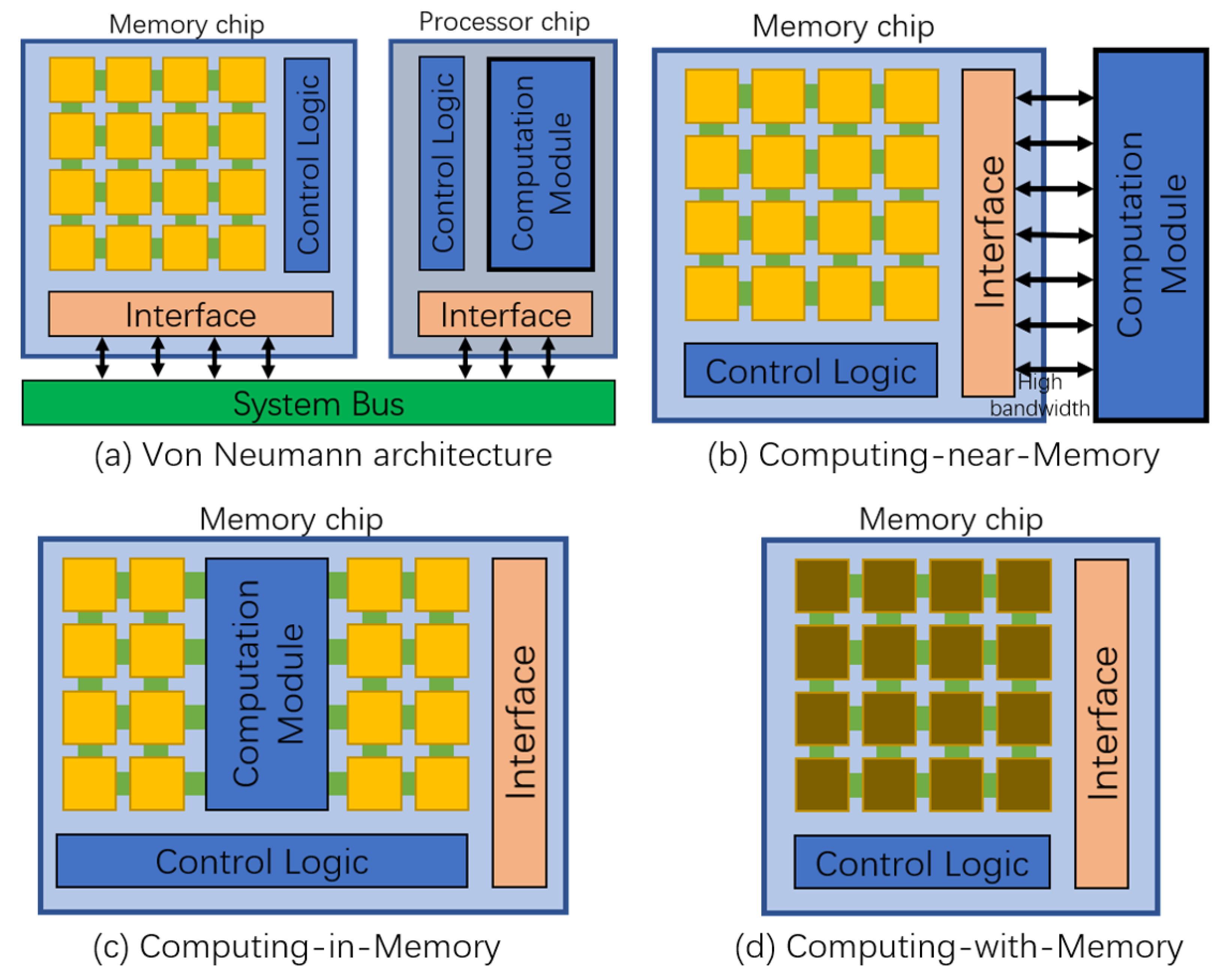
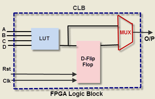
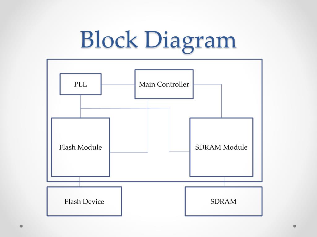
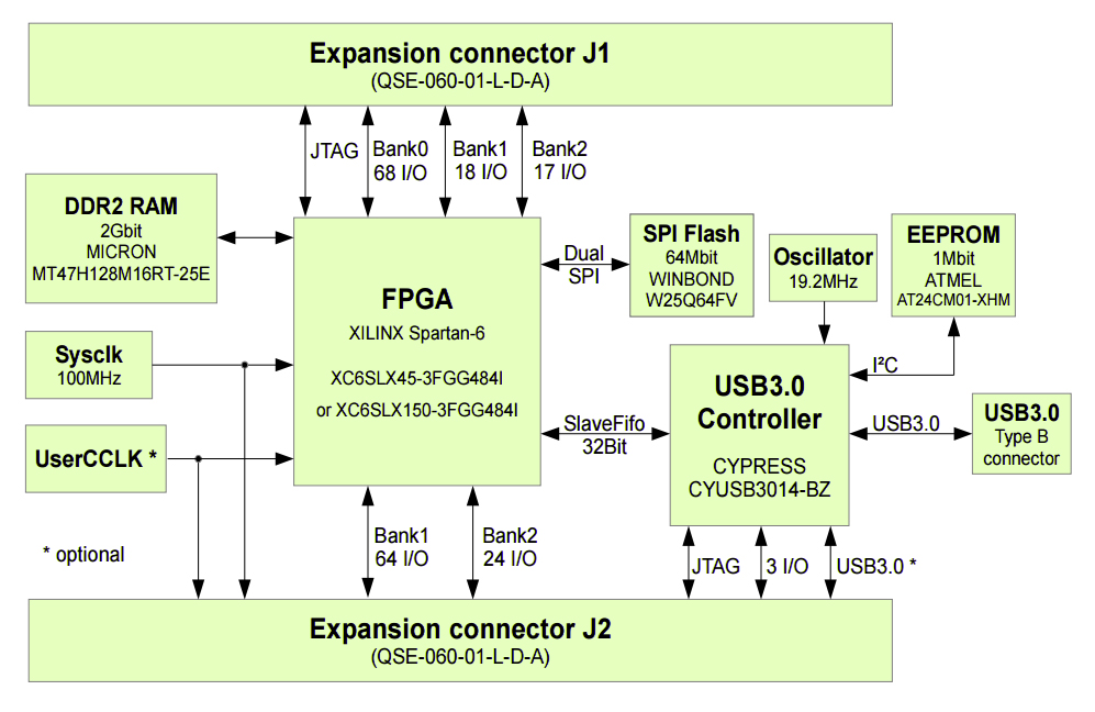
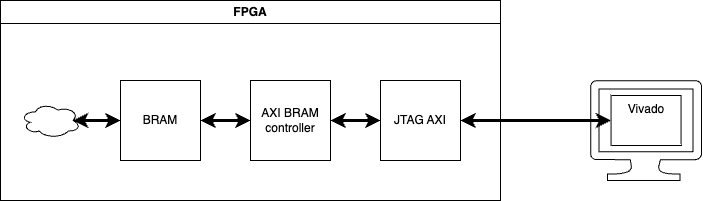
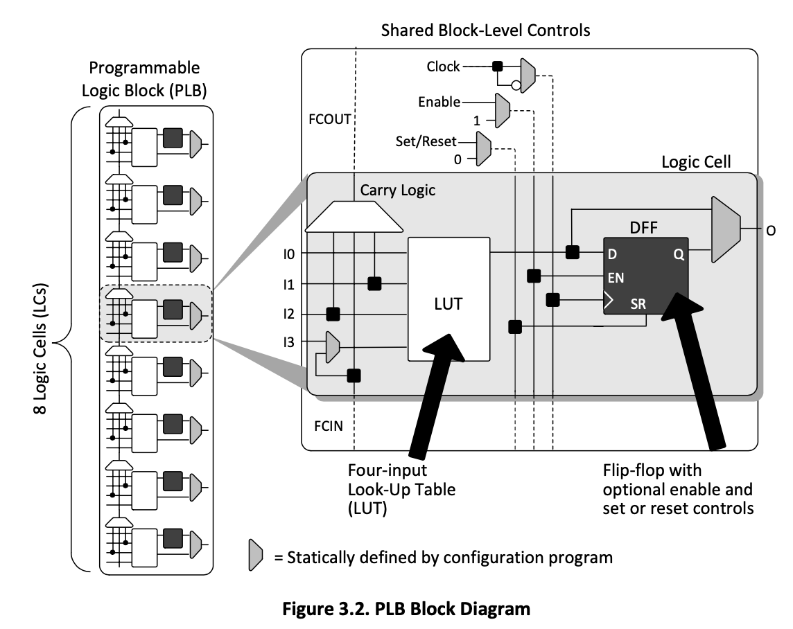
Fpga With Ram Block Diagram


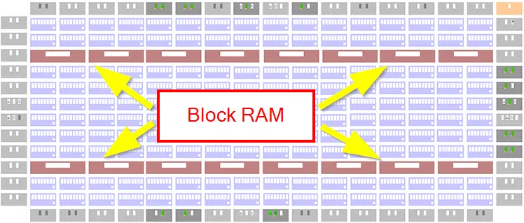


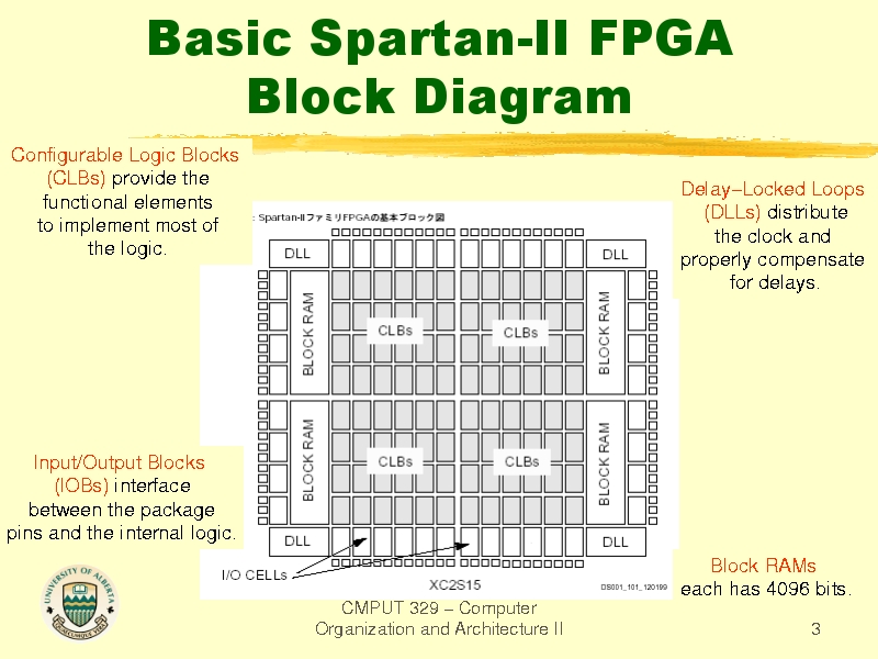


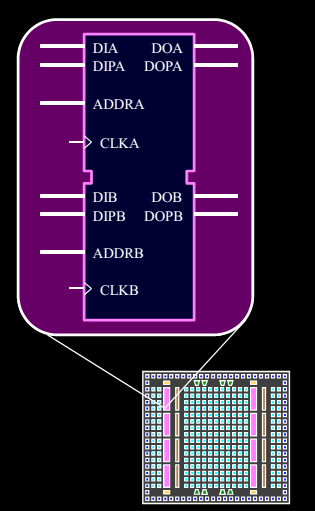


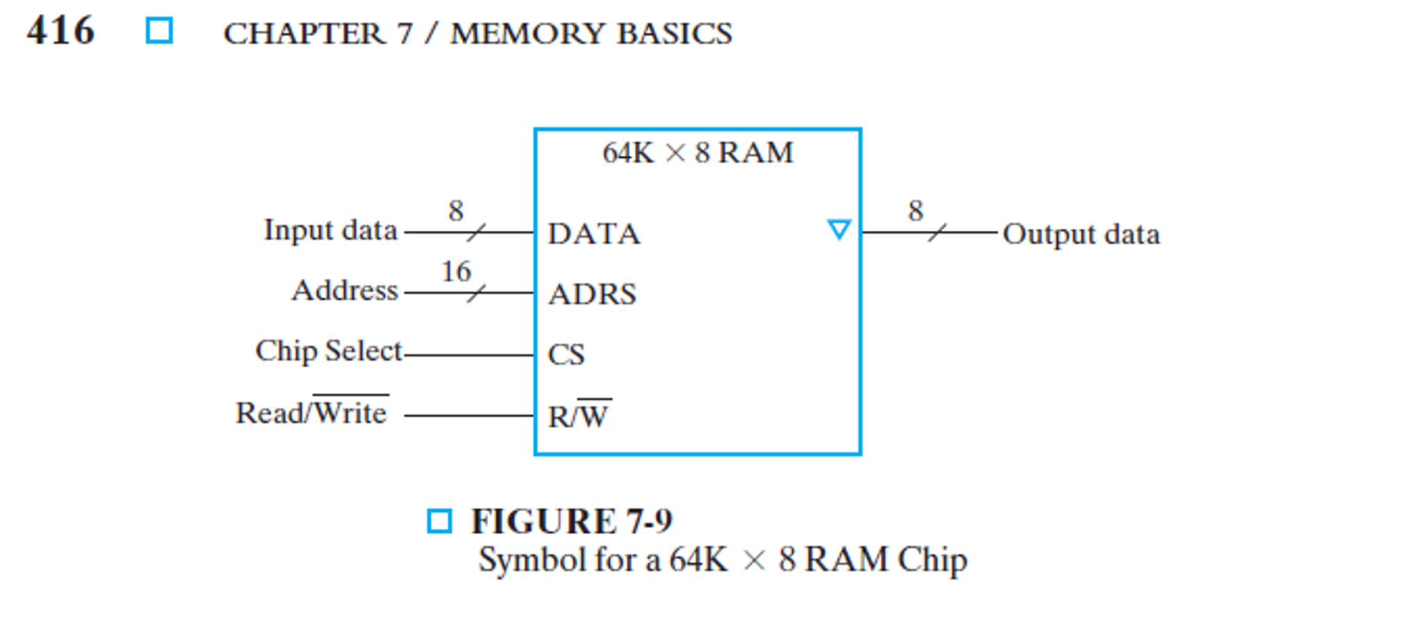


![Basic FPGA structure, from [5] | Download Scientific Diagram](https://www.researchgate.net/profile/Chris_Jackson15/publication/242531464/figure/fig10/AS:298450517282820@1448167556379/Proposed-shared-block-RAM-control-unit_Q320.jpg)


Discover destinations through vast arrays of journey-focused Fpga With Ram Block Diagram photographs. wanderlust-inspiring highlighting photography, images, and pictures. designed to inspire wanderlust and exploration. Browse our premium Fpga With Ram Block Diagram gallery featuring professionally curated photographs. Suitable for various applications including web design, social media, personal projects, and digital content creation All Fpga With Ram Block Diagram images are available in high resolution with professional-grade quality, optimized for both digital and print applications, and include comprehensive metadata for easy organization and usage. Discover the perfect Fpga With Ram Block Diagram images to enhance your visual communication needs. Advanced search capabilities make finding the perfect Fpga With Ram Block Diagram image effortless and efficient. Comprehensive tagging systems facilitate quick discovery of relevant Fpga With Ram Block Diagram content. The Fpga With Ram Block Diagram collection represents years of careful curation and professional standards. Diverse style options within the Fpga With Ram Block Diagram collection suit various aesthetic preferences. Cost-effective licensing makes professional Fpga With Ram Block Diagram photography accessible to all budgets. Professional licensing options accommodate both commercial and educational usage requirements. Reliable customer support ensures smooth experience throughout the Fpga With Ram Block Diagram selection process. Regular updates keep the Fpga With Ram Block Diagram collection current with contemporary trends and styles.