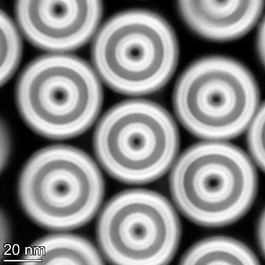
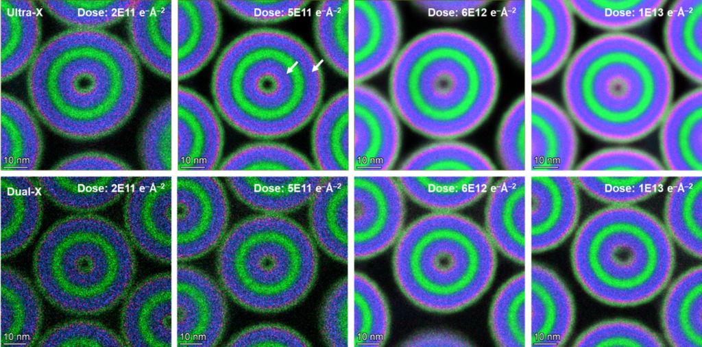
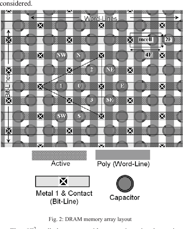
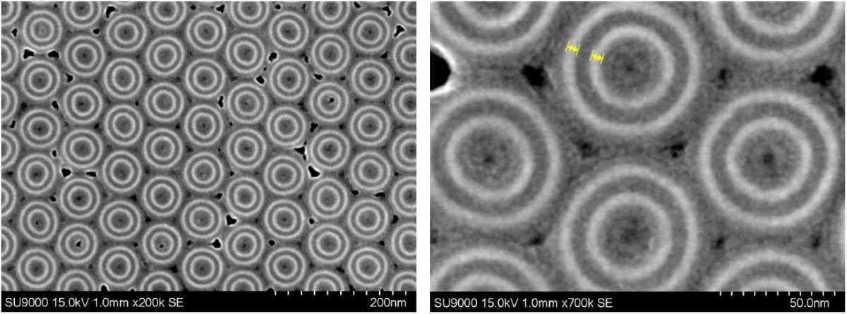
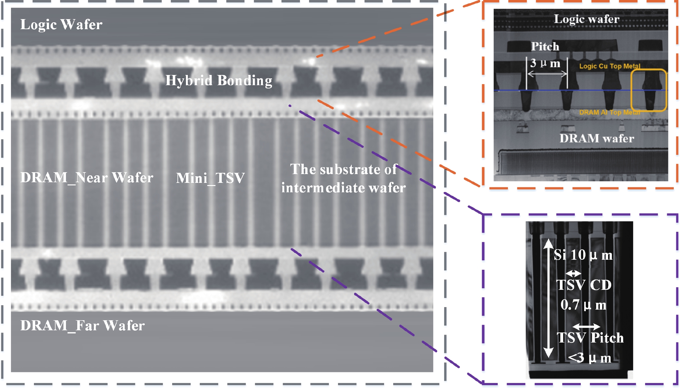
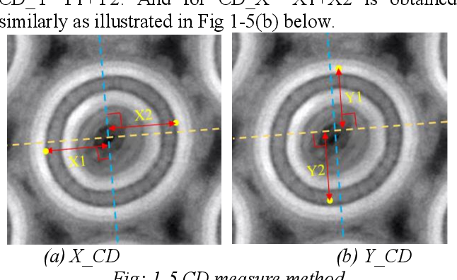
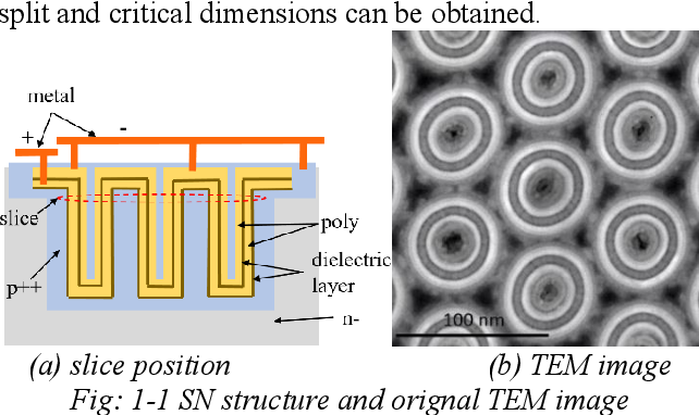
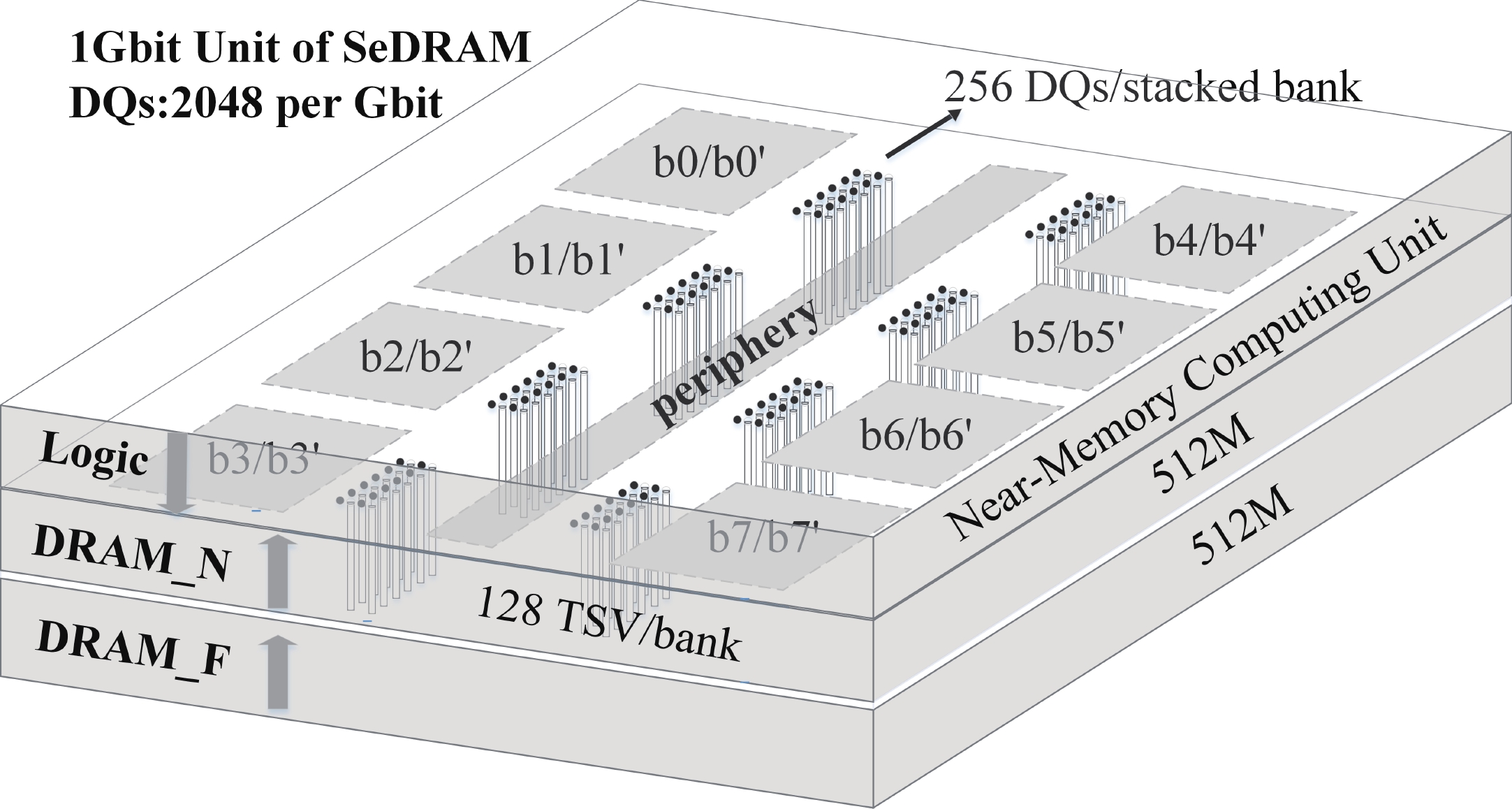
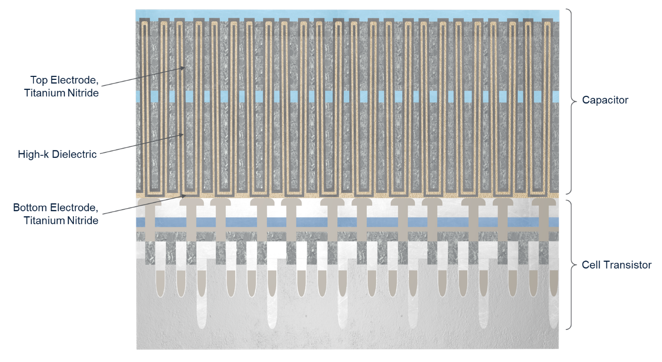
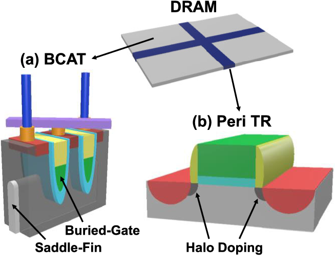
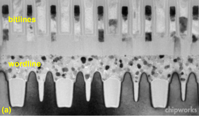
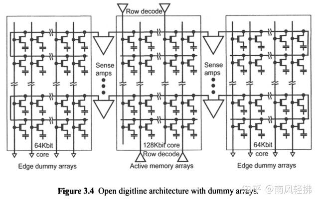
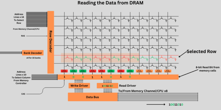
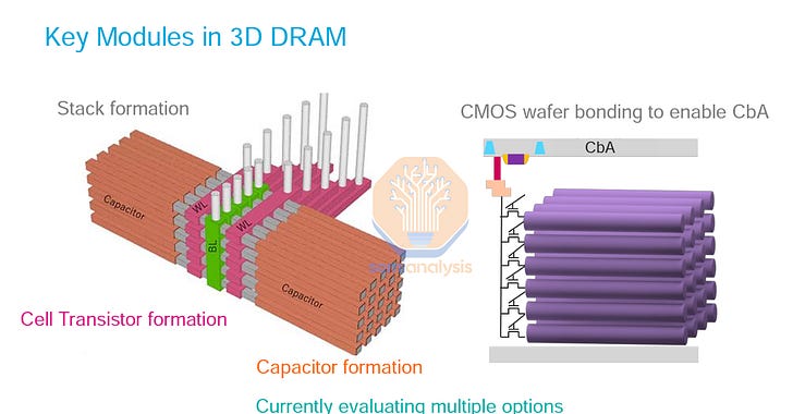
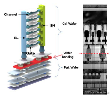
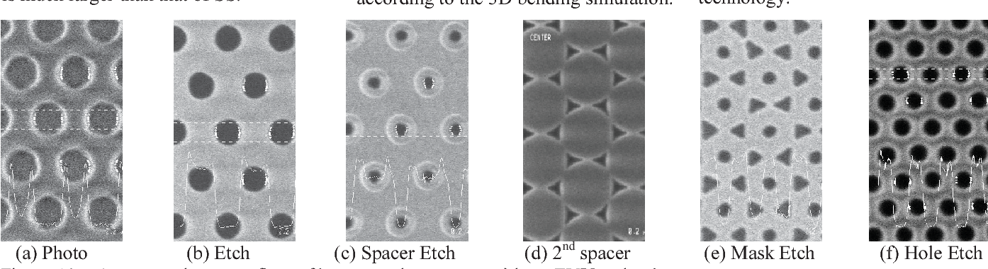
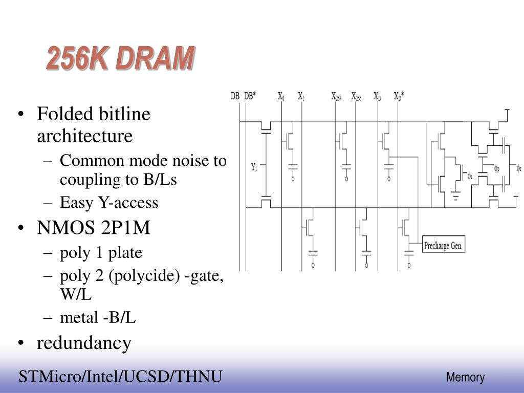
Dram Array Pattern Tem


![[Electronics] TEM sample prep of 1y nm DRAM - YouTube](https://i.ytimg.com/vi/11NsjuZ416M/maxresdefault.jpg)
![[Electronics] TEM of 1y nm DRAM (Dynamic Random Access Memory) - YouTube](https://i.ytimg.com/vi/w5uDapzjtFc/maxresdefault.jpg)


![[Electronics] Plan-view TEM/STEM of DRAM capacitors - YouTube](https://i.ytimg.com/vi/pZmBUN1uDPA/maxresdefault.jpg)
![[Electronics] FIB-SEM tomography of DRAM Memory Cell using orthogonally ...](https://i.ytimg.com/vi/Bln-v9LmZ3E/maxresdefault.jpg)


![[Electronics] Plane view SEM/STEM of DRAM capacitor - YouTube](https://i.ytimg.com/vi/do9U6kbmCug/maxresdefault.jpg)


![Hitachi Electron Microscope on LinkedIn: [Electronics] TEM of 1y nm ...](https://media.licdn.com/dms/image/C5605AQFm9-BI4jHqUg/videocover-high/0/1674197558030?e=2147483647&v=beta&t=c2pmL4xmbPgFpddarsWwjUTsfmQtVh7N2Y4bo1eVdoE)


![[PDF] Novel Dual Work Function Buried Channel Array Transistor Process ...](https://d3i71xaburhd42.cloudfront.net/da034b5c50a021b29a5a42878567d8b7e8cb1818/6-Figure4-1.png)


Discover the stunning beauty of minimalist Dram Array Pattern Tem with comprehensive galleries of clean images. highlighting the purity of photography, images, and pictures. ideal for clean and simple aesthetics. Our Dram Array Pattern Tem collection features high-quality images with excellent detail and clarity. Suitable for various applications including web design, social media, personal projects, and digital content creation All Dram Array Pattern Tem images are available in high resolution with professional-grade quality, optimized for both digital and print applications, and include comprehensive metadata for easy organization and usage. Explore the versatility of our Dram Array Pattern Tem collection for various creative and professional projects. The Dram Array Pattern Tem archive serves professionals, educators, and creatives across diverse industries. Reliable customer support ensures smooth experience throughout the Dram Array Pattern Tem selection process. Each image in our Dram Array Pattern Tem gallery undergoes rigorous quality assessment before inclusion. Time-saving browsing features help users locate ideal Dram Array Pattern Tem images quickly. Instant download capabilities enable immediate access to chosen Dram Array Pattern Tem images. Our Dram Array Pattern Tem database continuously expands with fresh, relevant content from skilled photographers. Diverse style options within the Dram Array Pattern Tem collection suit various aesthetic preferences.