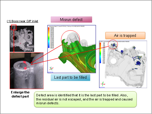
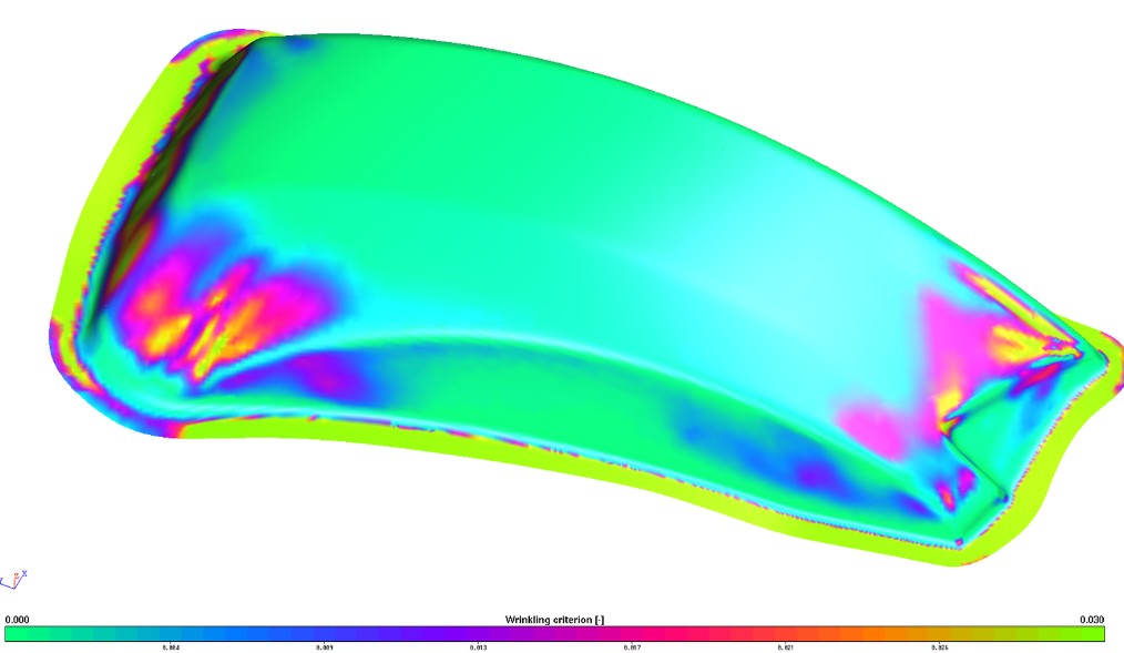
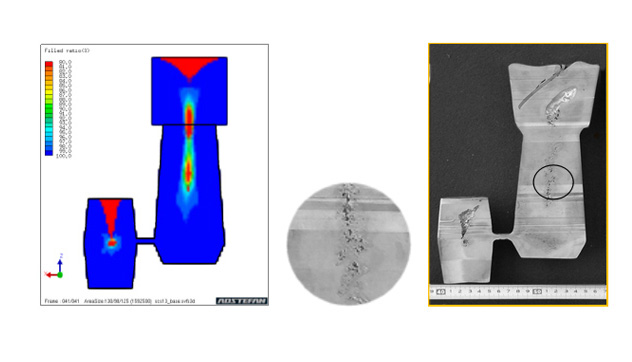
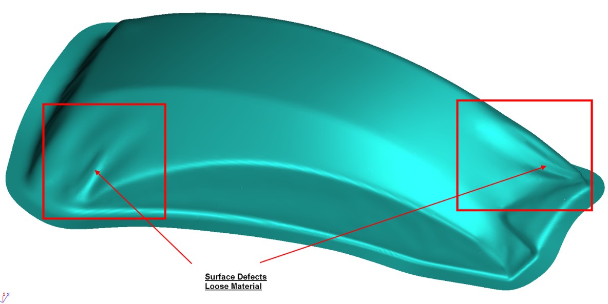
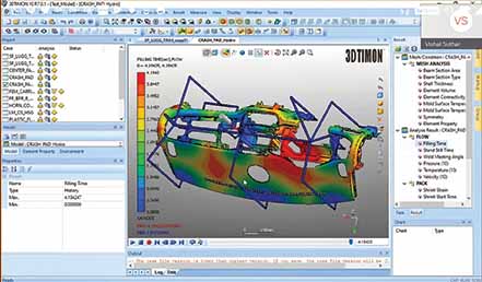
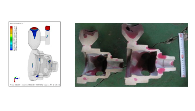
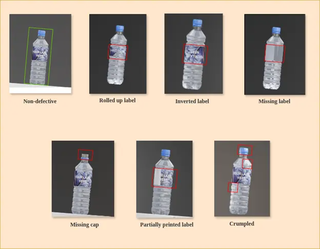
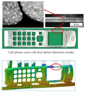
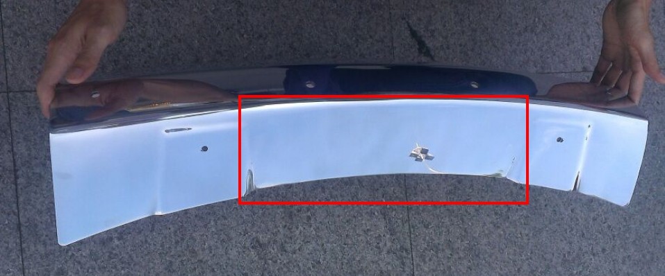
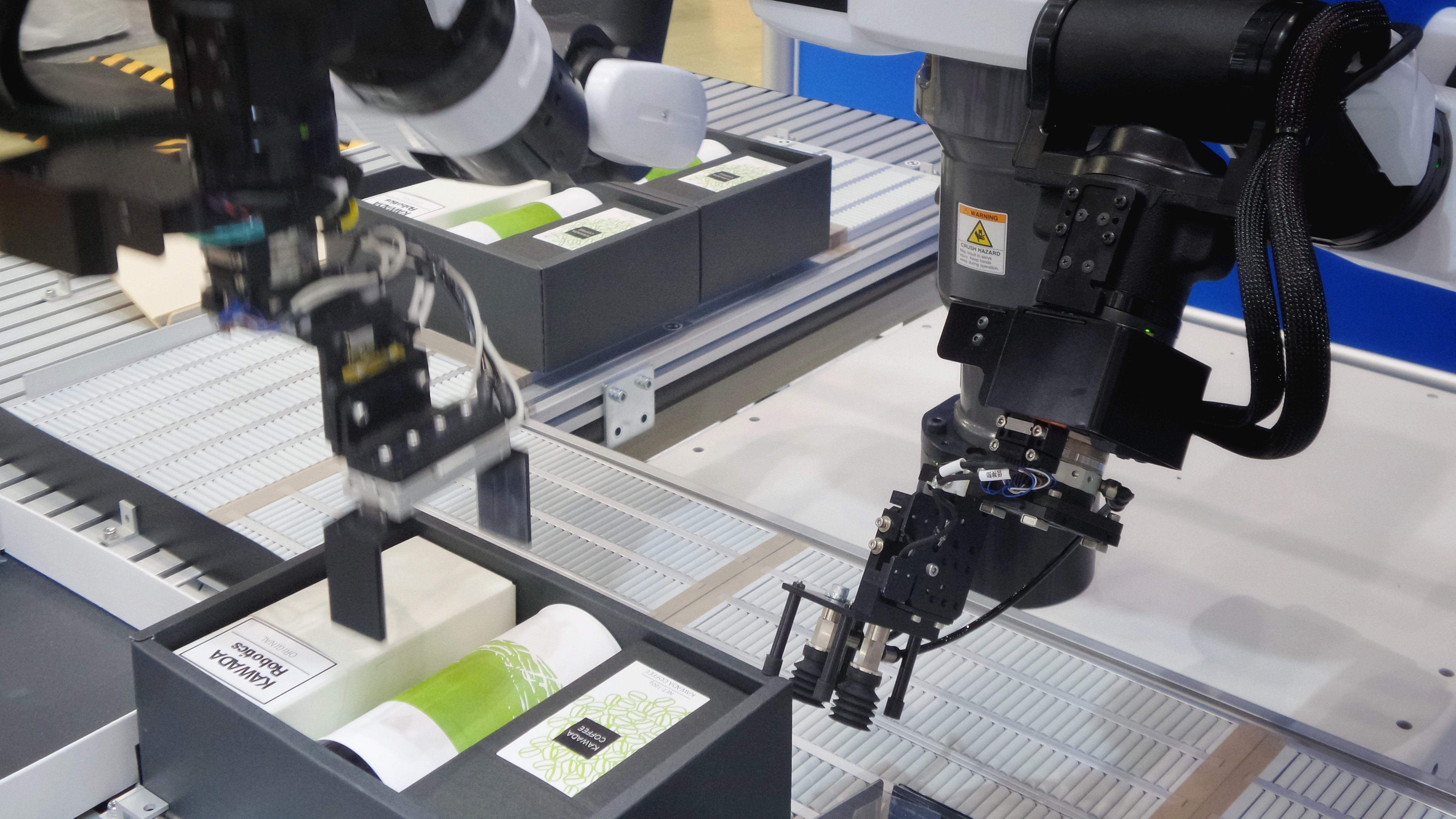
Defect Simulation


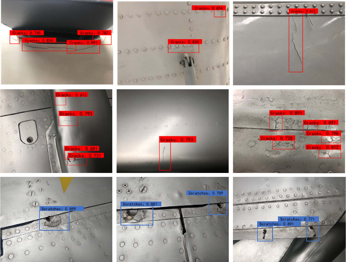
![A Complete Guide To Build Defect Detection Model [Updated]](https://cdn.labellerr.com/1Enhancing%20Safety%20in%20the%20Metal%20Industry%20with%20AI-Powered%20Defect%20Detection/11.webp)


![[논문 리뷰] Deep Learning-based Multi Project InP Wafer Simulation for ...](https://moonlight-paper-snapshot.s3.ap-northeast-2.amazonaws.com/arxiv/deep-learning-based-multi-project-inp-wafer-simulation-for-unsupervised-surface-defect-detection-3.png)

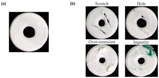
![Defect engineering for device application [19] | Download Scientific ...](https://www.researchgate.net/profile/Amall-Ramanathan/publication/323502329/figure/fig2/AS:599559461945344@1519957523009/Defect-engineering-for-device-application-19_Q320.jpg)


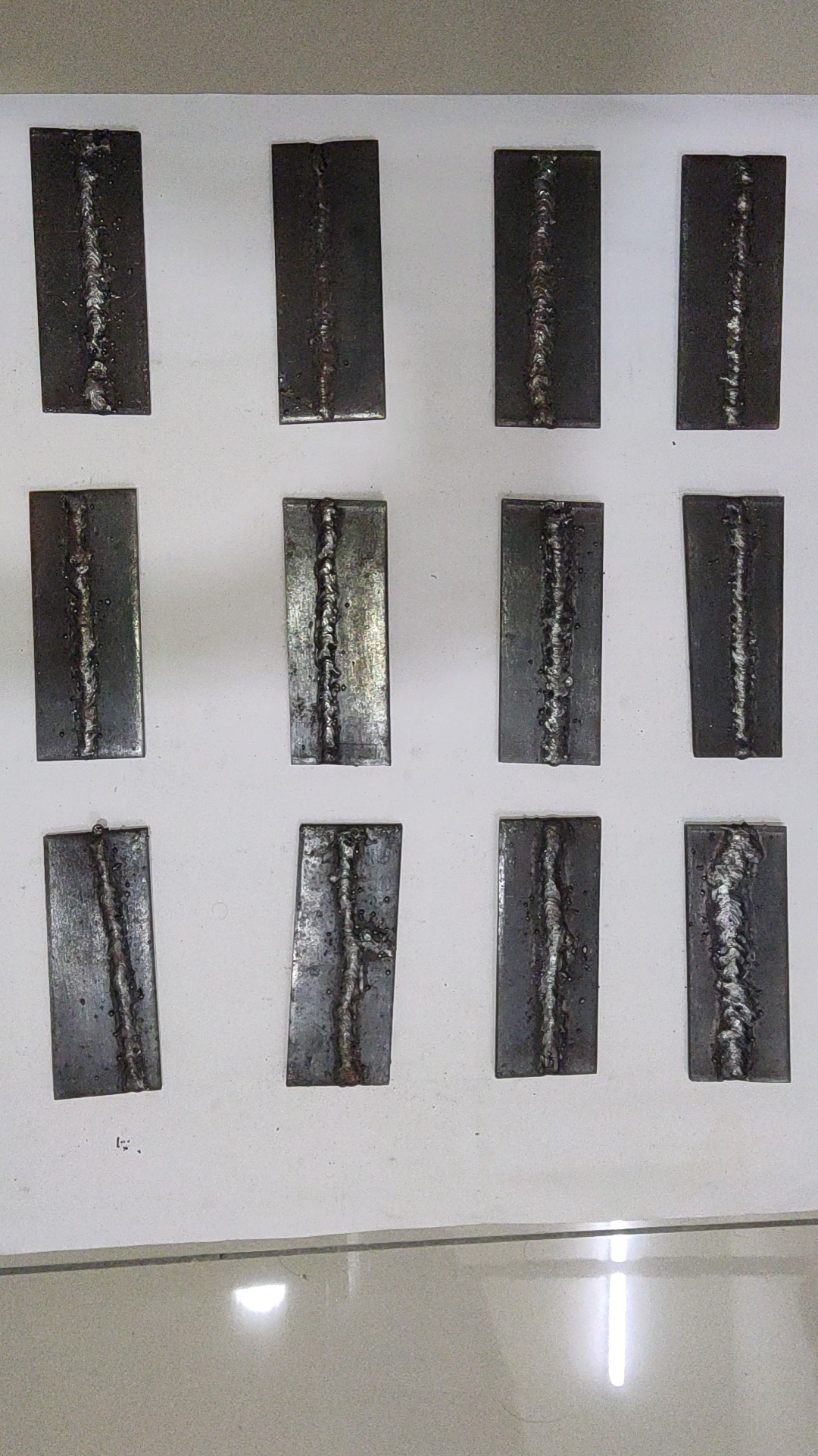


Examine the stunning technical aspects of Defect Simulation with vast arrays of detailed images. illustrating the mechanical aspects of photography, images, and pictures. ideal for engineering and scientific applications. Each Defect Simulation image is carefully selected for superior visual impact and professional quality. Suitable for various applications including web design, social media, personal projects, and digital content creation All Defect Simulation images are available in high resolution with professional-grade quality, optimized for both digital and print applications, and include comprehensive metadata for easy organization and usage. Explore the versatility of our Defect Simulation collection for various creative and professional projects. The Defect Simulation archive serves professionals, educators, and creatives across diverse industries. Instant download capabilities enable immediate access to chosen Defect Simulation images. Each image in our Defect Simulation gallery undergoes rigorous quality assessment before inclusion. Comprehensive tagging systems facilitate quick discovery of relevant Defect Simulation content. Our Defect Simulation database continuously expands with fresh, relevant content from skilled photographers. Advanced search capabilities make finding the perfect Defect Simulation image effortless and efficient. Cost-effective licensing makes professional Defect Simulation photography accessible to all budgets. Diverse style options within the Defect Simulation collection suit various aesthetic preferences. Multiple resolution options ensure optimal performance across different platforms and applications.