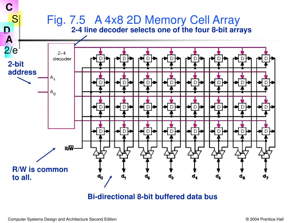
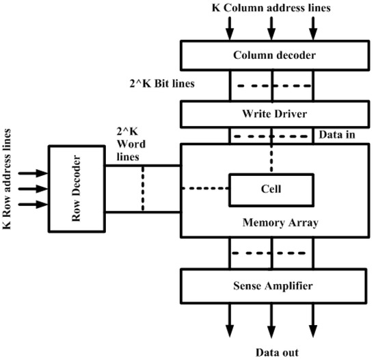
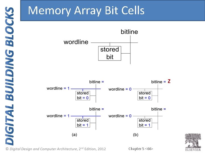
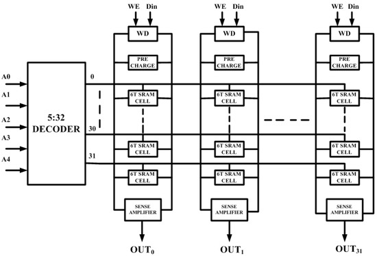
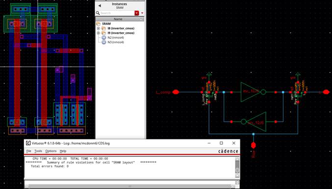
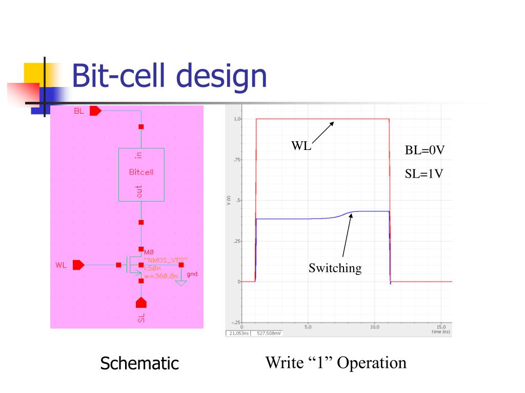
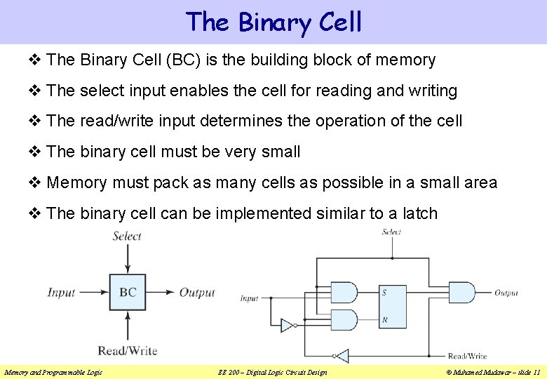
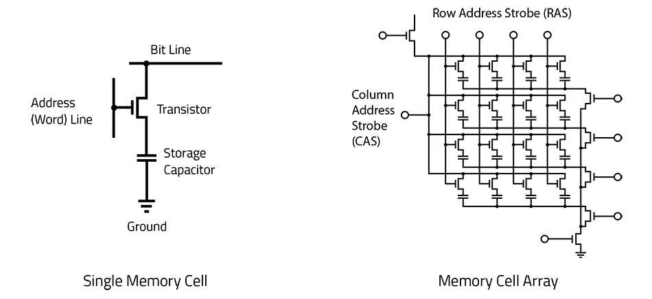
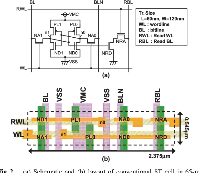
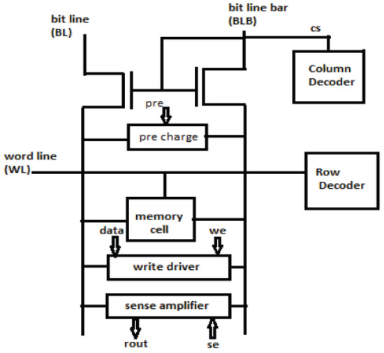
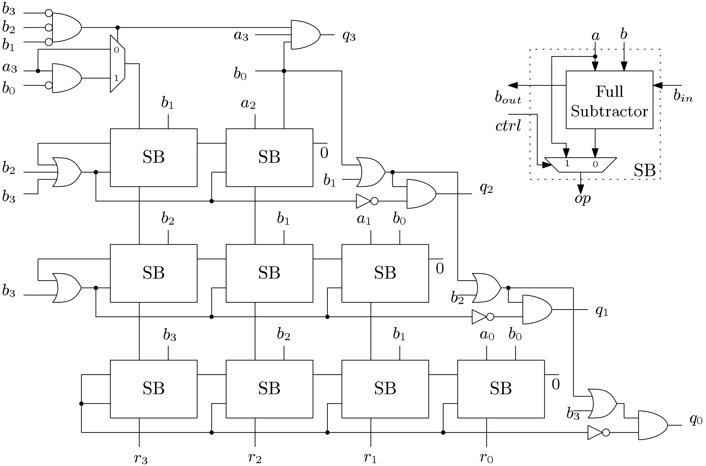
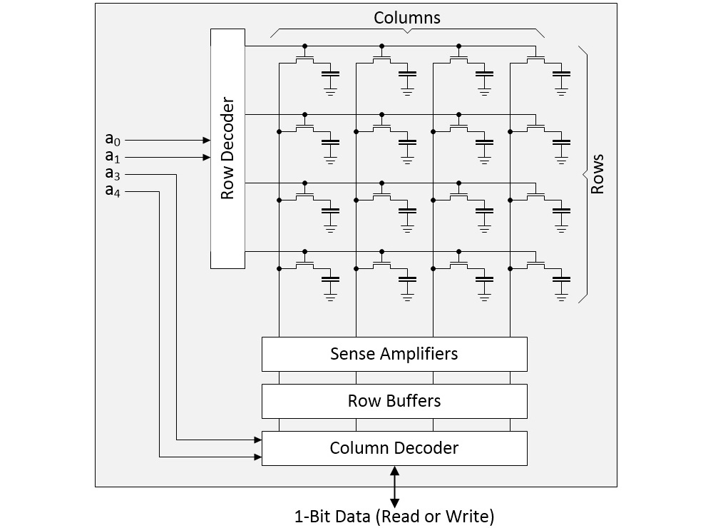
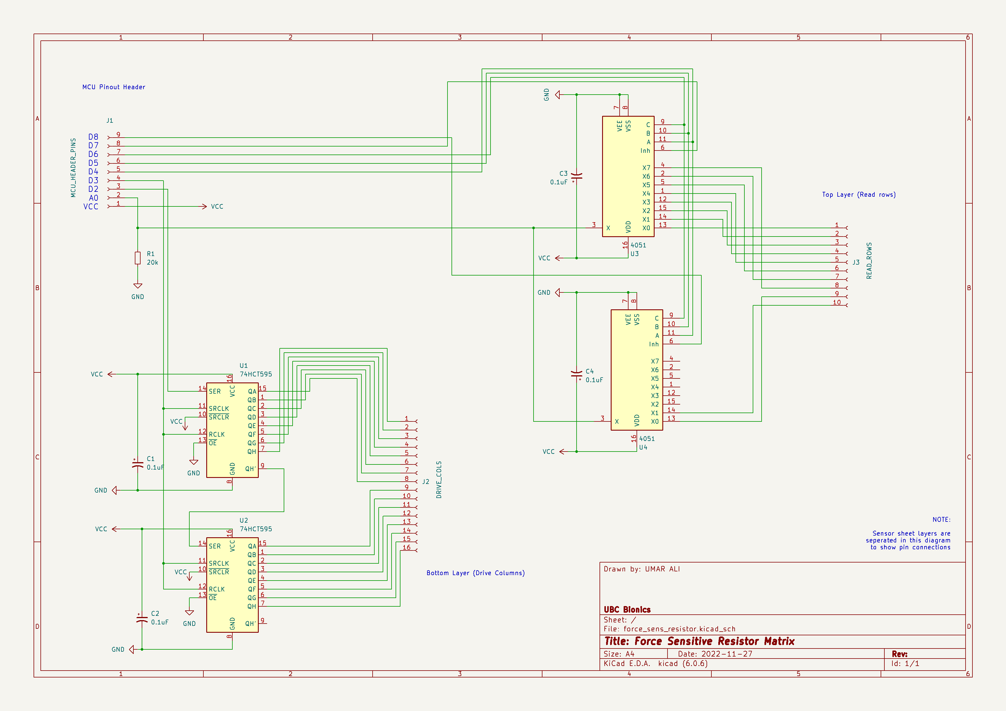
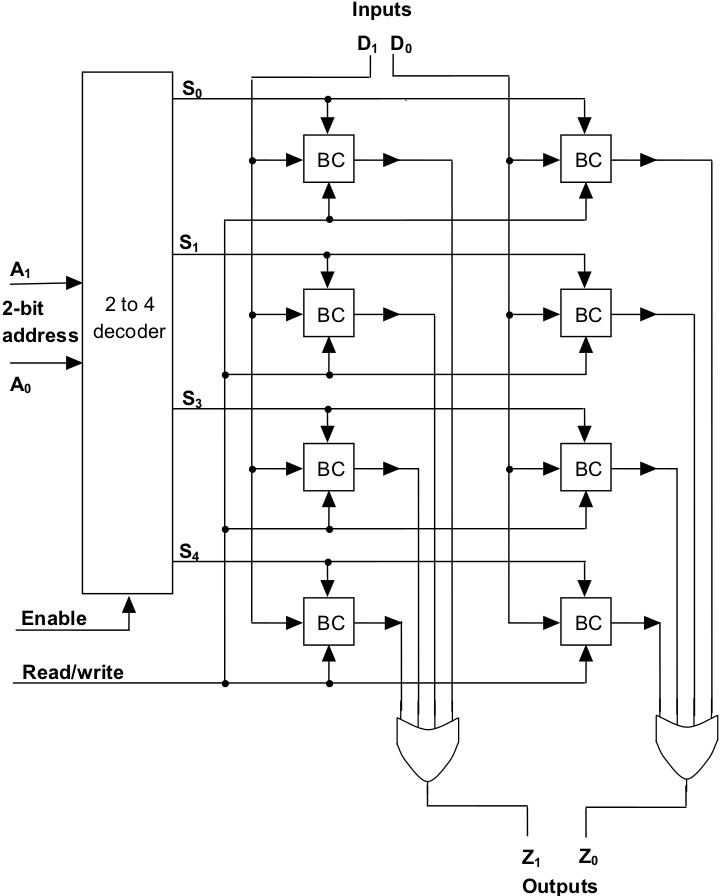
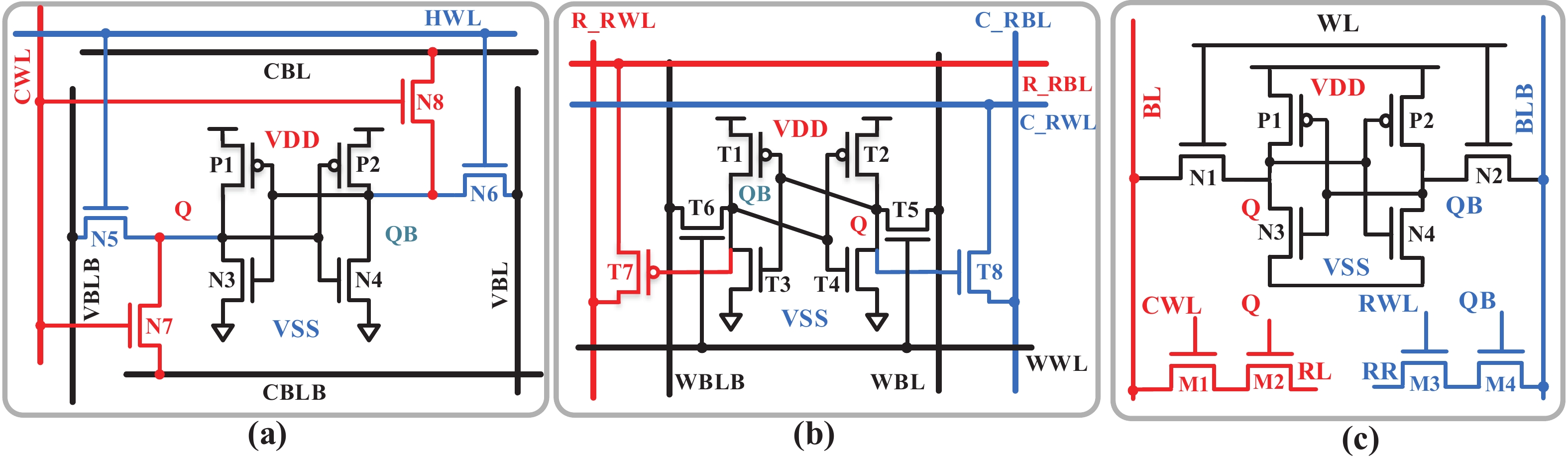
Bit Cell Matrix Example Schematic


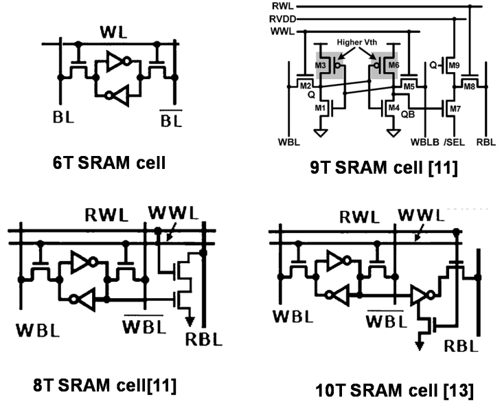
![(a) Bit-cell proposed by Jain et al. [26] which stores read-only and ...](https://www.researchgate.net/profile/Sparsh-Mittal-2/publication/329139565/figure/fig4/AS:695966885765120@1542942844415/a-Bit-cell-proposed-by-Jain-et-al-26-which-stores-read-only-and-programmable-data.png)


![(a) 8T-SRAM bit-cell in the design of Jaiswal et al. [32] (b) Config1 ...](https://www.researchgate.net/publication/351344022/figure/fig17/AS:1019968820875272@1620190925095/a-8T-SRAM-bit-cell-in-the-design-of-Jaiswal-et-al-32-b-Config1-and-c-Config2.png)


![Block diagram of 4×4-bit array multiplier [12] | Download Scientific ...](https://www.researchgate.net/profile/Navdeep-Goel/publication/264852676/figure/fig3/AS:527490422919169@1502774925159/Block-diagram-of-44-bit-array-multiplier-12.png)
![[Solved]: The diagram below represents a 4 times 4 NAND-base](https://media.cheggcdn.com/study/8f9/8f90e101-2cdf-4de9-9cb6-21f2d6786de4/image.jpg)


![The 8T bit-cell [4]. | Download Scientific Diagram](https://www.researchgate.net/publication/303509647/figure/fig1/AS:669976008609818@1536746136806/The-8T-bit-cell-4_Q640.jpg)


Document reality with our stunning Bit Cell Matrix Example Schematic collection of numerous authentic images. honestly portraying photography, images, and pictures. ideal for historical documentation and archives. Browse our premium Bit Cell Matrix Example Schematic gallery featuring professionally curated photographs. Suitable for various applications including web design, social media, personal projects, and digital content creation All Bit Cell Matrix Example Schematic images are available in high resolution with professional-grade quality, optimized for both digital and print applications, and include comprehensive metadata for easy organization and usage. Discover the perfect Bit Cell Matrix Example Schematic images to enhance your visual communication needs. Regular updates keep the Bit Cell Matrix Example Schematic collection current with contemporary trends and styles. The Bit Cell Matrix Example Schematic collection represents years of careful curation and professional standards. Reliable customer support ensures smooth experience throughout the Bit Cell Matrix Example Schematic selection process. Each image in our Bit Cell Matrix Example Schematic gallery undergoes rigorous quality assessment before inclusion. Whether for commercial projects or personal use, our Bit Cell Matrix Example Schematic collection delivers consistent excellence. Time-saving browsing features help users locate ideal Bit Cell Matrix Example Schematic images quickly. Diverse style options within the Bit Cell Matrix Example Schematic collection suit various aesthetic preferences.