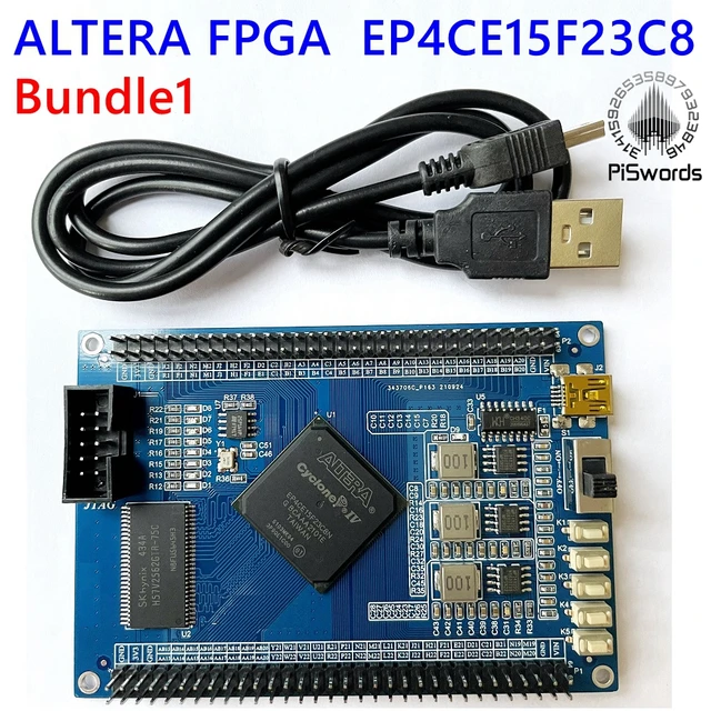
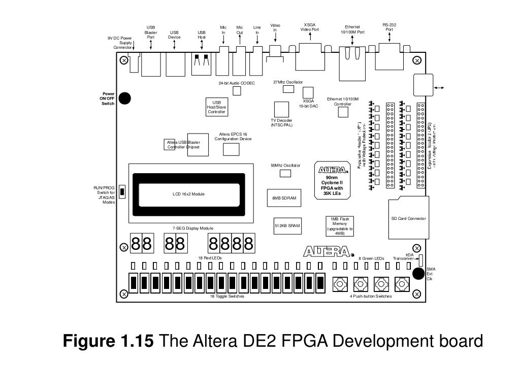
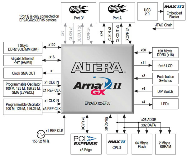
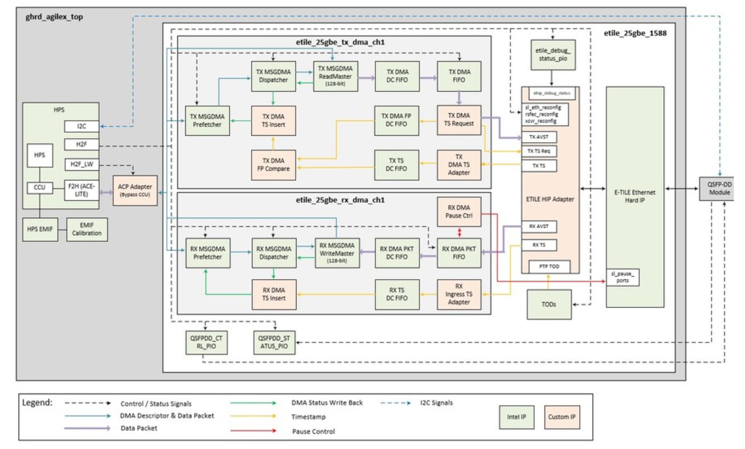
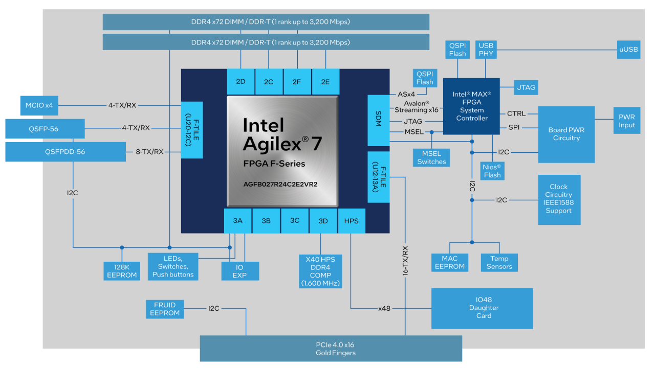
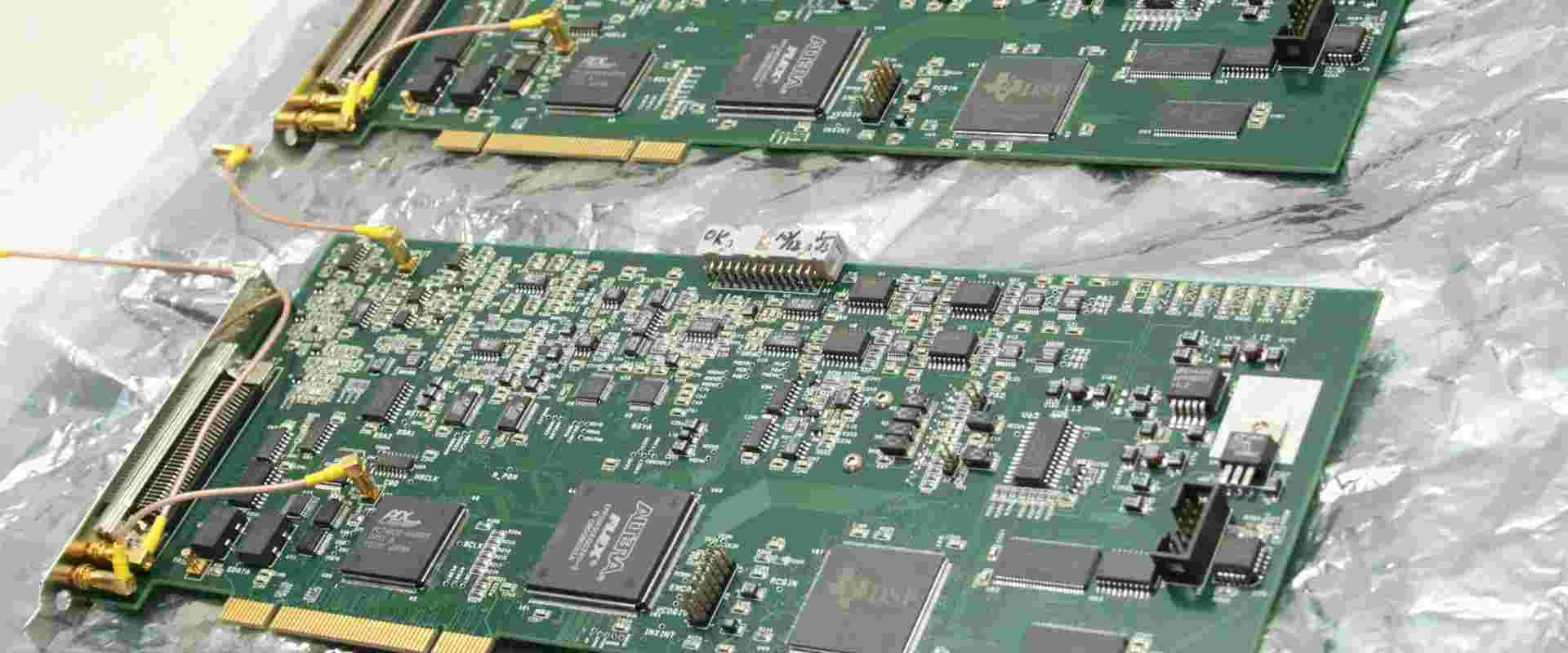
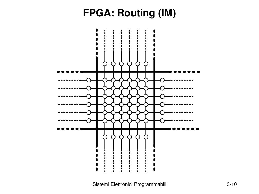
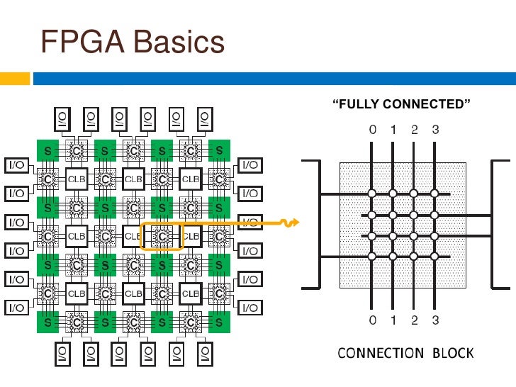
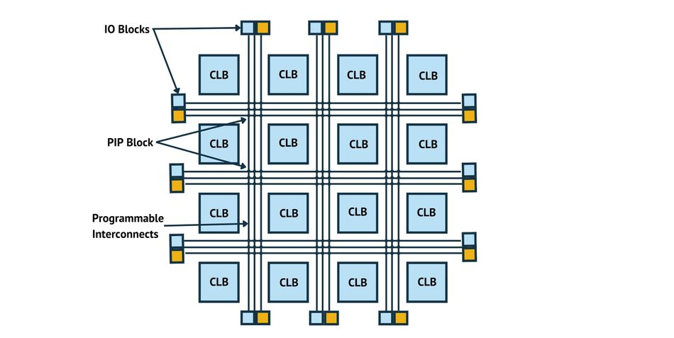
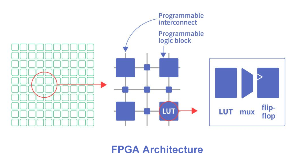
Altera Routing Diagram Fpga


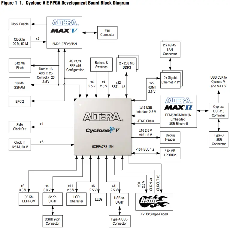
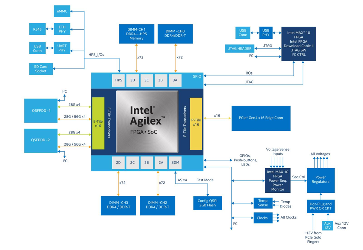
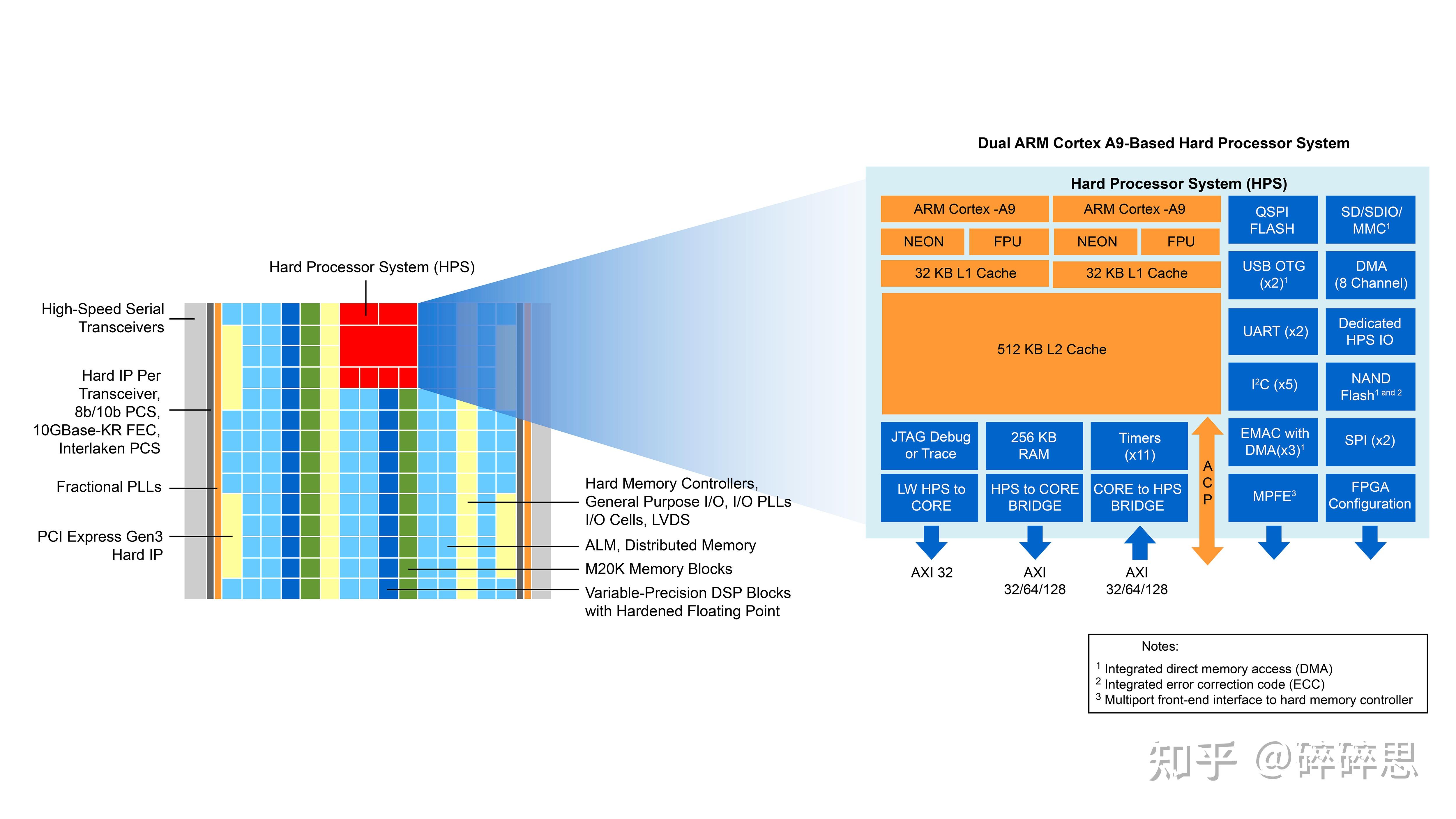
![Altera SoC FPGA Device Block Diagram [1, pp. 1-1] | Download Scientific ...](https://www.researchgate.net/profile/Mariano-Ruiz-2/publication/315690131/figure/fig1/AS:477233962852354@1490792851689/Altera-SoC-FPGA-Device-Block-Diagram-1-pp-1-1_Q640.jpg)


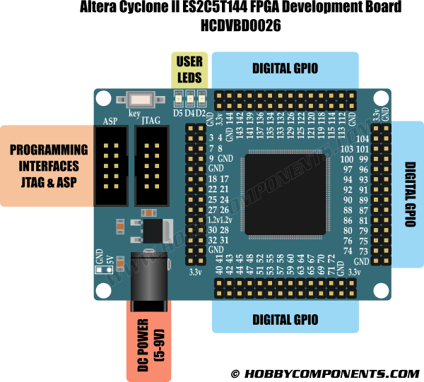
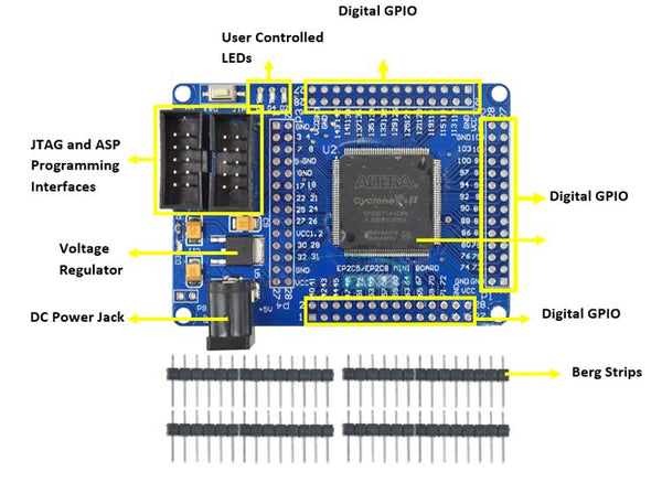
![Altera cyclone IV 4CE115 FPGA device [13]. | Download Scientific Diagram](https://www.researchgate.net/publication/361630571/figure/fig3/AS:11431281099636414@1669288854284/Altera-cyclone-IV-4CE115-FPGA-device-13.png)


%20internal%20architecture%20diagram%20showing%20a%20LUT%20(Look-Up%20Table),%20D-FF%20(D%20Flip-Flop),%20and%20MUX%20(Multiplexer)%20with%20inputs%20A,%20B,%20C,%20D,%20Rst,%20Clk%20and%20an%20output.png)


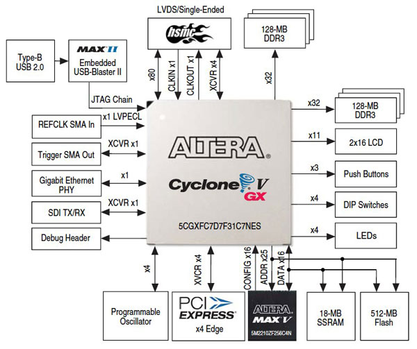

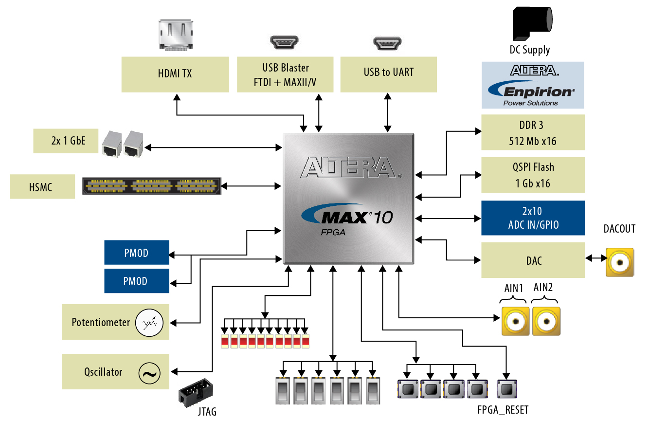
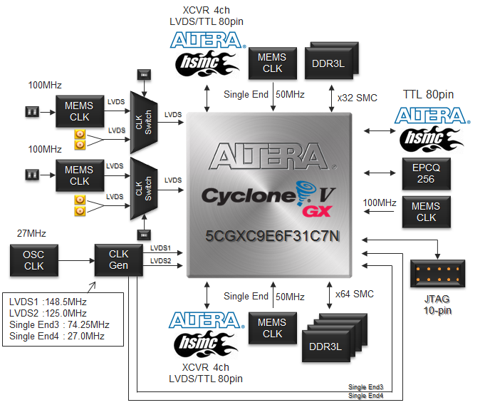
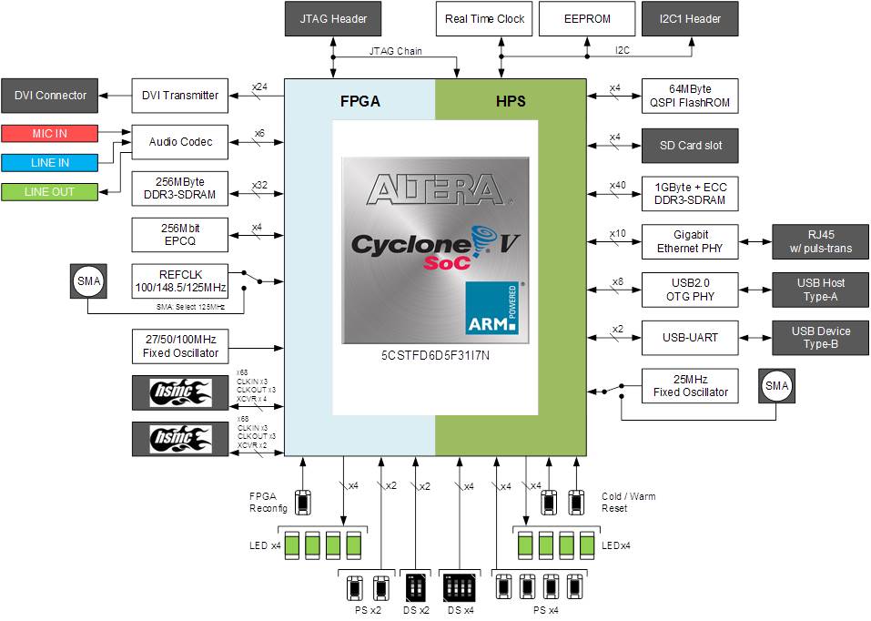
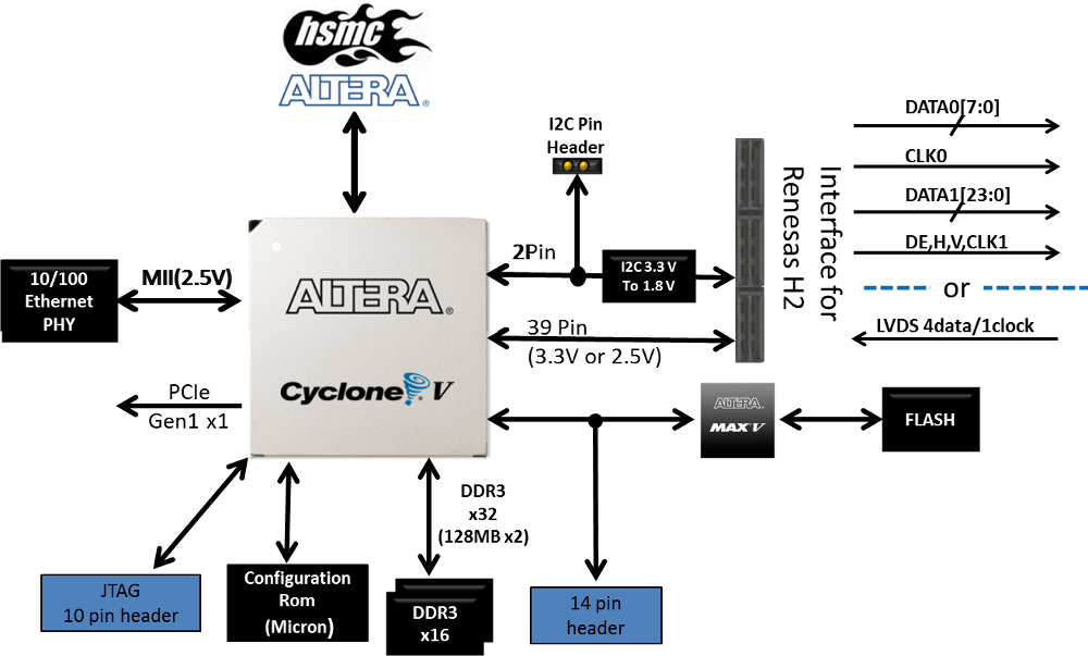
![[Altera] do I need to use the HPS of my board ? : r/FPGA](https://www.terasic.com.tw/attachment/archive/941/image/Blockdiagram.jpg)

Journey into the realm of Altera Routing Diagram Fpga through our curated selection of numerous stunning photographs. showcasing photography, images, and pictures. designed for diverse creative and educational needs. Each Altera Routing Diagram Fpga image is carefully selected for superior visual impact and professional quality. Suitable for various applications including web design, social media, personal projects, and digital content creation All Altera Routing Diagram Fpga images are available in high resolution with professional-grade quality, optimized for both digital and print applications, and include comprehensive metadata for easy organization and usage. Our Altera Routing Diagram Fpga gallery offers diverse visual resources to bring your ideas to life. Our Altera Routing Diagram Fpga database continuously expands with fresh, relevant content from skilled photographers. Time-saving browsing features help users locate ideal Altera Routing Diagram Fpga images quickly. Instant download capabilities enable immediate access to chosen Altera Routing Diagram Fpga images. The Altera Routing Diagram Fpga archive serves professionals, educators, and creatives across diverse industries. The Altera Routing Diagram Fpga collection represents years of careful curation and professional standards. Comprehensive tagging systems facilitate quick discovery of relevant Altera Routing Diagram Fpga content. Professional licensing options accommodate both commercial and educational usage requirements. Each image in our Altera Routing Diagram Fpga gallery undergoes rigorous quality assessment before inclusion.